


Quick Research
Generate reliable direction feasibility study reports for your R&D in just a few steps.

Technical Q&A
Discover and master advanced knowledge NOW. Basics, ideas, possibilities, all at once.

Find Solutions
As an expert in R&D theories, this can generate solutions to your technical problems instantly.

Evaluate Feasibility
Analyze your overall solution with one click, know your potential R&D risks in advance.

Monitor Landscape
Get weekly tech updates, stay abreast of the latest tech innovations and key insights.
A method for growing large-area mos2 thin films
A thin-film growth and large-area technology, applied in the direction of gaseous chemical plating, metal material coating process, coating, etc., can solve the problem of scarcity of MoS2 single crystal preparation technology, and achieve easy repeatability, low cost, and facilitate industrialization The effect of production
- Summary
- Abstract
- Description
- Claims
- Application Information
AI Technical Summary
Problems solved by technology
Method used
Image


Examples
Embodiment 1
[0021] Embodiments of the present invention provide a method for synthesizing large-area MoS 2 The preparation method of thin film, concrete steps are carried out as follows;
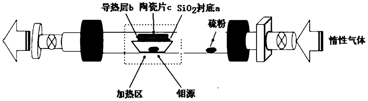
[0022] Put sulfur powder and molybdenum trioxide into figure 1 Placed in the corresponding position as shown, wherein molybdenum trioxide is 0.1 mole, sulfur powder B is 0.2 mole; SiO 2 The substrate a, the heat-conducting gold foil layer b, and the ceramic sheet c are stacked in sequence and placed on the top of the molybdenum source. The temperature of the body was raised to 700°C and kept for 20 minutes. After the reaction was complete, the sample was taken out for characterization. The prepared MoS 2 A film with a film size of 150 microns and a film thickness of 3 nm.
[0023] figure 2 Represents the MoS prepared in Example 1 2 Optical microscope photographs of the films, from figure 2 It can be seen that the prepared film has a uniform morphology;
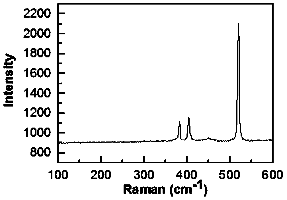
[0024] After Raman characterization of t...
Embodiment 2
[0027] Put sulfur powder and molybdenum trioxide into figure 1 Placed in the corresponding position as shown, where molybdenum source A is 0.1 mole, sulfur source B is 0.2 mole; SiO 2 The substrate a, the heat-conducting gold foil layer b, and the ceramic sheet c are stacked in sequence and placed above the molybdenum source. The temperature of the body was raised to 800°C, and the temperature was kept for 30 minutes. After the reaction was complete, the sample was taken out for characterization. The prepared MoS 2 The film size is 300 microns, the film thickness is 5 nanometers, and the prepared film has uniform morphology.
PUM
| Property | Measurement | Unit |
|---|---|---|
| Size | aaaaa | aaaaa |
| Thickness | aaaaa | aaaaa |
| Size | aaaaa | aaaaa |
Abstract
Description
Claims
Application Information
 - R&D Engineer
- R&D Manager
- IP Professional
- Industry Leading Data Capabilities
- Powerful AI technology
- Patent DNA Extraction
Browse by: Latest US Patents, China's latest patents, Technical Efficacy Thesaurus, Application Domain, Technology Topic, Popular Technical Reports.
© 2024 PatSnap. All rights reserved.Legal|Privacy policy|Modern Slavery Act Transparency Statement|Sitemap|About US| Contact US: help@patsnap.com