Disordered netty carbon nanotube based p-n junction diode and preparation method thereof

A carbon nanotube and carbon nanotube film technology, which is applied in the field of p-n junction diodes and their preparation, can solve problems such as complex processes, and achieve the effects of stable performance and excellent rectification characteristics

Inactive Publication Date: 2016-04-27
SHANGHAI JIAO TONG UNIV
View PDF4 Cites 0 Cited by
  • Summary
  • Abstract
  • Description
  • Claims
  • Application Information

AI Technical Summary

Problems solved by technology

But this technology needs to make two different metal electrodes, which makes the process more complicated

Method used


Image

  • Disordered netty carbon nanotube based p-n junction diode and preparation method thereof
  • Disordered netty carbon nanotube based p-n junction diode and preparation method thereof

Examples


Embodiment 1

[0027] This embodiment includes the following steps:

[0028] The first step is to use electrostatic self-assembly technology to self-assemble a layer with a density of 1.5 μm on the surface of the silicon wafer -2 disordered carbon nanotube films.

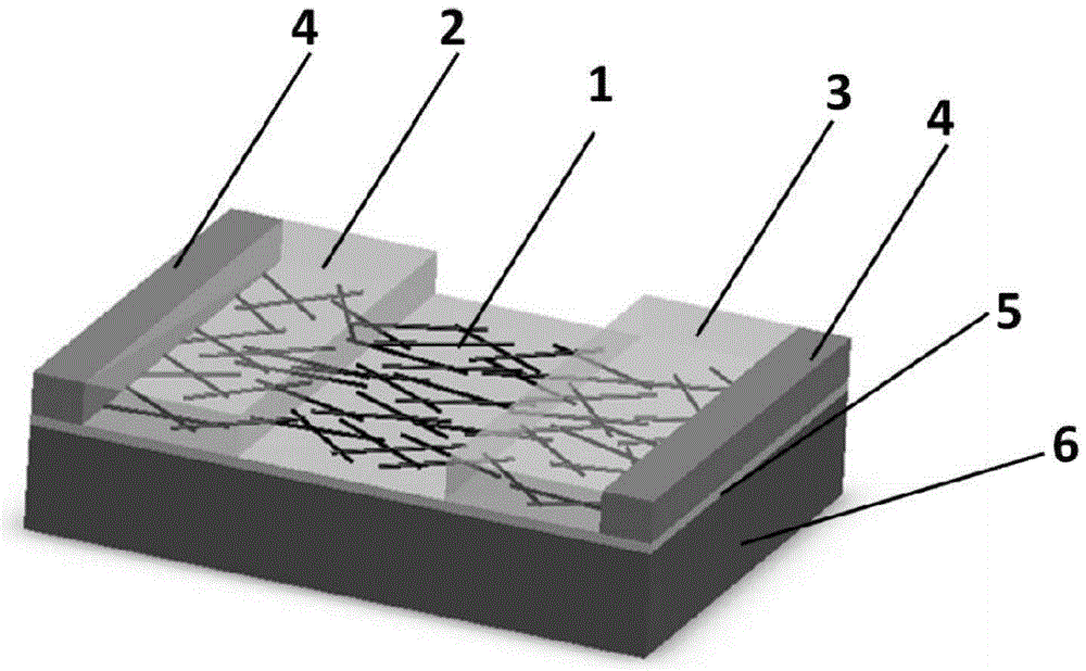
[0029] In the second step, Au symmetric electrodes (such as figure 1 ), the electrode width is 5 μm, and the distance between opposite electrodes is 6 μm.

[0030] In the third step, the excess carbon nanotubes beside the channel of the amorphous network carbon nanotubes are etched away by ion etching technology.

[0031] In the fourth step, the electron beam photoresist is coated on the substrate, and one end of the disordered network carbon nanotube is exposed by opening a window with a window size of 5 μm*3 μm by using the electron beam lithography technique. The exposed end of the disordered network carbon nanotube channel will be exposed to the air after being developed and fixed. The unexposed end will be protected by ph...

Embodiment 2

[0036] This embodiment includes the following steps:

[0037] The first step is to use electrostatic self-assembly technology to self-assemble a layer with a density of 1.5 μm on the surface of the silicon wafer -2 disordered carbon nanotube films.

[0038] In the second step, electron beam lithography and magnetron sputtering techniques are used to fabricate Au symmetrical electrodes at both ends of the carbon nanotubes, with an electrode width of 5 μm and a distance between opposite electrodes of 6 μm.

[0039] In the third step, the excess carbon nanotubes beside the channel of the disordered network carbon nanotubes are etched away by ion etching technology.

[0040] In the fourth step, the electron beam photoresist is coated on the substrate, and one end of the carbon nanotube is exposed to a window by using the electron beam lithography technology, and the window size is 5 μm*2 μm. The exposed portion (5 μm*2 μm) of the disordered network carbon nanotube channel will b...

Embodiment 3

[0044] This embodiment includes the following steps:

[0045] The first step is to use electrostatic self-assembly technology to self-assemble on the surface of silicon wafers with a density of 1.5 μm -2 disordered carbon nanotube films.

[0046] In the second step, electron beam lithography and magnetron sputtering techniques are used to fabricate Au symmetrical electrodes at both ends of the carbon nanotubes, with an electrode width of 5 μm and a distance between opposite electrodes of 6 μm.


PUM

PropertyMeasurementUnit
diameteraaaaaaaaaa
lengthaaaaaaaaaa
widthaaaaaaaaaa

Abstract

The invention relates to a disordered netty carbon nanotube based p-n junction diode and a preparation method thereof. The preparation method comprises the following steps: manufacturing Au electrodes through electron beam lithography and magnetron sputtering at two ends of a carbon nanotube thin film on a substrate, then soaking one end of the carbon nanotube thin film in a triethyloxonium hexachloroantimonate solution to form a p-type doping area and soaking the other end of the carbon nanotube thin film in a polyethyleneimine solution to form an n-type doping area after photoresist spinning and selective exposing, and preparing to obtain the p-n junction diode. Through the adoption of disordered netty carbon nanotubes, the prepared and obtained device has good rectification characteristic, and is stable in performances in room temperature air. The performances of the diode can be freely regulated and controlled by changing the density of the disordered netty carbon nanotubes and the structure size and doping parameters of the device.

Description

technical field [0001] The invention relates to a diode manufacturing technology, in particular to a p-n junction diode based on disordered network carbon nanotubes and a preparation method thereof. Background technique [0002] Carbon nanotubes are one-dimensional nanomaterials with excellent mechanical and electronic properties, and are considered to be the first choice for making future nanodevices. At present, diodes based on single carbon nanotubes have been successfully produced. However, in practical applications, it is technically challenging to assemble a single carbon nanotube onto two electrodes. Moreover, the repeatability of the performance of a single device is also limited by the carbon nanotube purification process. Disordered network carbon nanotubes have the characteristics of simple preparation process and repeatability of device performance, so they can be used to replace single carbon nanotube devices in practical applications. [0003] Similar to sin...

Claims


Application Information

Patent Timeline
Patent Type & Authority Applications(China)
IPC IPC(8): H01L51/40H01L51/05H01L51/30H01L31/18
CPCH01L31/18H10K85/221H10K10/20Y02E10/549Y02P70/50
Inventor 陈长鑫刘晓东
Owner SHANGHAI JIAO TONG UNIV
Why Eureka
Try Eureka