Electrochromic multi-layered transparent conductive thin film and preparation method therefor

A transparent conductive film, electrochromic technology, applied in cable/conductor manufacturing, conductive layer on insulating carrier, coating and other directions, can solve problems such as hindering Ag electron exchange, film loss of conductivity, etc., to achieve fast film growth rate , The effect of high coloring efficiency and good electrical conductivity

Inactive Publication Date: 2016-05-04
UNIV OF ELECTRONICS SCI & TECH OF CHINA
View PDF4 Cites 12 Cited by
  • Summary
  • Abstract
  • Description
  • Claims
  • Application Information

AI Technical Summary

Problems solved by technology

WO 3 The work functions of Ag and Ag are 5.24eV and 4.4ev, respectively, which can meet this requirement; 3 , it is easily oxidized by high-energy oxygen ions to form Ag x O, whose work function is about 5.47-5.61eV, forms a surface barrier at the interface, hindering Ag and WO 3 The exchange of electrons between the films makes the film lose conductivity

Method used


Image

  • Electrochromic multi-layered transparent conductive thin film and preparation method therefor
  • Electrochromic multi-layered transparent conductive thin film and preparation method therefor
  • Electrochromic multi-layered transparent conductive thin film and preparation method therefor

Examples


Embodiment 1

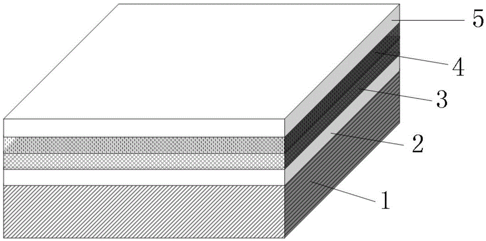
[0027] In this embodiment, an electrochromic multilayer transparent conductive film is provided, and its structure is as follows: figure 1 As shown, including the substrate, the first WO 3 Thin film layer, Ag conductive layer, W buffer layer and second WO 3 Thin film layer, first WO 3 Thin film layer, Ag conductive layer, W buffer layer and second WO 3 The thickness of the film layer is 45nm, 10-12nm, 2-3nm and 45nm respectively, and the substrate adopts standard electronic white glass.

[0028] Its preparation method comprises the following steps:

[0029] 1) Prepare the first WO 3 Thin film layer: evacuate the vacuum chamber (~5.0×10 -4 Pa), then pass in argon, adjust the argon pressure (1.0Pa), then turn on the radio frequency power switch, and then pass in oxygen after the target glows, adjust the flow of argon and oxygen (40:60sccm), so that the air pressure in the vacuum chamber is constant (4.0×10 -1 Pa), adjust the sputtering power (200W), and then perform pre-s...

Embodiment 2

[0035] The electrochromic multilayer transparent conductive film with the same structure as in Example 1 was prepared by the following steps, specifically:

[0036] 1) Prepare the first WO 3 Thin film layer: evacuate the vacuum chamber (~5.0×10 -4 Pa), then pass in argon, adjust the argon pressure (1.0Pa), then turn on the radio frequency power switch, and then pass in oxygen after the target glows, adjust the flow of argon and oxygen (40:60sccm), so that the air pressure in the vacuum chamber is constant (4.0×10 -1 Pa), adjust the sputtering power (200W), and then perform pre-sputtering cleaning (10 minutes) on the W target, then turn the substrate platform to the top of the target, adjust the sputtering time (18 minutes), and place on the glass substrate WO 3 film;

[0037] 2) Prepare the Ag conductive layer: adjust the argon flow rate (60sccm) to fix the air pressure in the vacuum chamber (3.4×10 -1 Pa), and then turn on the DC power switch. After the target glows, adj...

Embodiment 3

[0041] The electrochromic multilayer transparent conductive film with the same structure as in Example 1 was prepared by the following steps, specifically:

[0042] 1) Prepare the first WO 3 Thin film layer: evacuate the vacuum chamber (~5.0×10 -4 Pa), then pass in argon, adjust the argon pressure (1.0Pa), then turn on the radio frequency power switch, and then pass in oxygen after the target glows, adjust the flow of argon and oxygen (40:60sccm), so that the air pressure in the vacuum chamber is constant (4.0×10 -1 Pa), adjust the sputtering power (200W), and then perform pre-sputtering cleaning (10 minutes) on the W target, then turn the substrate platform to the top of the target, adjust the sputtering time (18 minutes), and place on the glass substrate WO 3 film;

[0043] 2) Prepare the Ag conductive layer: adjust the argon flow rate (60sccm) to fix the air pressure in the vacuum chamber (3.4×10 -1 Pa), and then turn on the DC power switch. After the target glows, adj...


PUM

PropertyMeasurementUnit
thicknessaaaaaaaaaa
electron work functionaaaaaaaaaa

Abstract

The invention relates to a thin film and a preparation method therefor, and provides an electrochromic multi-layered transparent conductive thin film and a preparation method therefor. The multi-layered transparent conductive thin film comprises a substrate, a first WO3 thin film layer, an Ag conductive layer, a W buffer layer and a second WO3 thin film arranged from upper to lower in sequence; the preparation method comprises the steps of preparing the first WO3 thin film layer on the substrate through a reactive sputtering method; then preparing the Ag conductive layer and the W buffer layer on the surface of the first WO3 thin film layer through a direct current sputtering method and a magnetron sputtering method separately; and finally preparing the second WO3 thin film layer on the surface of the W film layer through the reactive sputtering method. The multi-layered transparent conductive thin film structure and the preparation process are optimized to prepare the electrochromic multi-layered transparent conductive thin film through the sputtering method; and the thin film has the advantages of high transmittance within a visible light range, high conductivity, large adjustment range for the visible light transmittance, high coloring efficiency, high cycling stability, environment friendliness and the like.

Description

technical field [0001] The invention relates to a film and a preparation method thereof, in particular to an electrochromic multilayer stack structure transparent conductive film and a preparation method thereof. Background technique [0002] Transparent conductive film is a photoelectric material that combines optical transparency and conductivity. Due to its excellent photoelectric properties, it has become a research hotspot and frontier topic in recent years. It can be widely used in solar cells, electrochromic, LED, TFT , LCD and touch screen and other fields. The most commonly used transparent conductive material is indium tin oxide (ITO), but due to the scarcity and rapid consumption of indium metal, the cost continues to rise, so it is urgent to find a relatively cheap alternative material. Among them, the dielectric-metal-dielectric (DMD) structure has excellent optical, electrical and structural properties (such as high electrical conductivity close to metal mater...

Claims


Application Information

Patent Timeline
Patent Type & Authority Applications(China)
IPC IPC(8): H01B5/14H01B13/00C23C14/35C23C14/08C23C14/18C23C14/16
CPCC23C14/0036C23C14/083C23C14/165C23C14/185C23C14/35H01B5/14H01B13/00
Inventor 尹伊李春兰长勇郭华阳
Owner UNIV OF ELECTRONICS SCI & TECH OF CHINA
Why Eureka
Try Eureka