Heat-conducting bonding pad and package structure of QFP chip with heat-conducting bonding pad

A technology for thermal pads and pads, which is used in semiconductor devices, semiconductor/solid-state device components, electrical components, etc., can solve the problems of poor thermal conductivity of thermal pads, improve the welding effect, reduce air bubbles, and ensure the welding effect. Effect

Inactive Publication Date: 2016-05-04
ZHUHAI GREE REFRIGERATION TECH CENT OF ENERGY SAVING & ENVIRONMENTAL PROTECTION
View PDF10 Cites 11 Cited by
  • Summary
  • Abstract
  • Description
  • Claims
  • Application Information

AI Technical Summary

Problems solved by technology

[0006] The main purpose of the present invention is to provide a heat conduction pad and a packaging structure of a QFP chip with it, to solve the problem of poor heat conduction effect of the heat conduction pad in the prior art

Method used


Image

  • Heat-conducting bonding pad and package structure of QFP chip with heat-conducting bonding pad
  • Heat-conducting bonding pad and package structure of QFP chip with heat-conducting bonding pad
  • Heat-conducting bonding pad and package structure of QFP chip with heat-conducting bonding pad

Examples


Embodiment 1

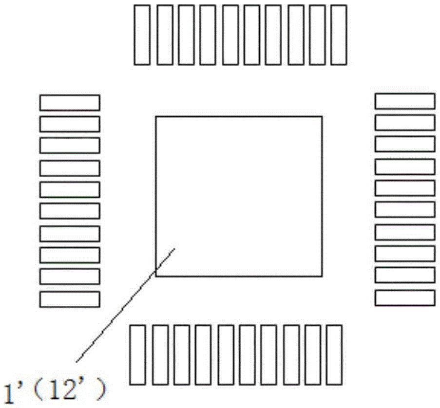
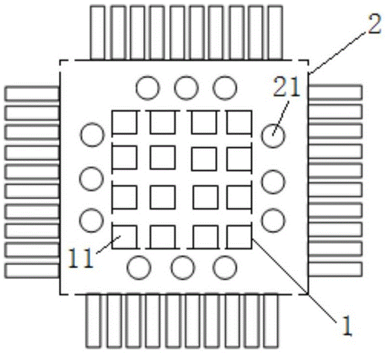
[0046] use has image 3 The heat conduction pad of the structure shown is used as the heat conduction pad of the packaging structure to package the QFP chip. The pad part is a square with a side length of 50 mils, and the distance between adjacent pad parts is 20 mils. The shortest distance of the area is 20mils, and the diameter of the vent hole is 30mils.

Embodiment 2

[0048] use has image 3 The heat conduction pad of the structure shown is used as the heat conduction pad of the packaging structure to package the QFP chip. The pad part is a square with a side length of 40 mils, and the distance between adjacent pad parts is 25 mils. The shortest distance of the area is 15mils, and the diameter of the vent hole is 20mils.

Embodiment 3

[0050] use has image 3 The heat conduction pad of the structure shown is used as the heat conduction pad of the packaging structure to package the QFP chip. The pad part is a square with a side length of 60 mils, and the distance between adjacent pad parts is 15 mils. The shortest distance of the area is 25mils, and the diameter of the vent hole is 40mils.


PUM


Abstract

The invention provides a heat-conducting bonding pad and a package structure of a QFP chip with the heat-conducting bonding pad. The heat-conducting bonding pad comprises a bonding pad region and a peripheral region, wherein the bonding pad region is provided with a plurality of bonding pad parts which are arranged in an array; and gaps are formed among the bonding pad parts. The bonding pad parts of the heat-conducting bonding pad are arranged in the array and are isolated from one another, and the area of the bonding pad parts is greatly reduced, so that, on one hand, the escape path of a gas generated by soldering flux pyrolysis in a solder paste in a high-temperature welding process is shortened; and on the other hand, the gaps between the adjacent bonding pad parts provide channels for escape of the gas; the gas can timely escape; the area and the quantity of bubbles are effectively reduced; the condition that the chip has enough heat radiating area is ensured; and the heat radiating effect is improved. Meanwhile, the effective area of a conductor formed by the bonding pad is increased, so that the grounding impedance of the chip is reduced; and the reliability of the chip is improved. The welding effect of the heat-conducting bonding pad is improved; and excessive floating of the chip is avoided, so that the welding reliability of peripheral pins is improved.

Description

technical field [0001] The invention relates to the field of chip packaging, in particular, to a heat-conducting pad and a packaging structure of a QFP chip having the same. Background technique [0002] Modern electronic packaging devices are developing towards high density, high integration and miniaturization, and QFP packaging (Quad Flat Package, four-sided flat packaging) occupies a mainstream position in chip packaging technology. At present, some highly integrated QFP package chips, such as TMS320F28377 produced by TI, have a pad for heat dissipation and grounding at the bottom of the chip in order to have a good heat dissipation and grounding effect. The role of the pad is to realize the electrical connection and mechanical connection between the chip and the external circuit, and between components, so its reliability is particularly important. The thermal stress and alternating cycles caused by the power cycle of the chip will lead to thermal fatigue of the pad, t...

Claims


Application Information

Patent Timeline
Patent Type & Authority Applications(China)
IPC IPC(8): H01L23/367H01L23/467H01L23/488
CPCH01L23/3677H01L23/467H01L23/488
Inventor 谭章德康燕施现伟张东盛
Owner ZHUHAI GREE REFRIGERATION TECH CENT OF ENERGY SAVING & ENVIRONMENTAL PROTECTION
Why Eureka
Try Eureka