Finned-type field effect transistor and fabrication method thereof

A fin-type field effect and transistor technology, which is applied in semiconductor/solid-state device manufacturing, semiconductor devices, electrical components, etc., can solve the problems of self-heating effect, high cost, poor thermal conductivity of buried oxide layer, etc., and avoid self-heating effect , cost control, and the effect of reducing leakage current

Inactive Publication Date: 2016-05-04
SHANGHAI INTEGRATED CIRCUIT RES & DEV CENT +1
View PDF6 Cites 4 Cited by
  • Summary
  • Abstract
  • Description
  • Claims
  • Application Information

AI Technical Summary

Problems solved by technology

But the disadvantages are also obvious: the cost of silicon wafers on SOI substrates is much higher than that of single crystal silicon substrates, and the buried oxide layer of SOI substrates has poor thermal conductivity, which is prone to self-heating effects

Method used


Image

  • Finned-type field effect transistor and fabrication method thereof
  • Finned-type field effect transistor and fabrication method thereof
  • Finned-type field effect transistor and fabrication method thereof

Examples


Embodiment Construction

[0031] In order to make the content of the present invention clearer and easier to understand, the content of the present invention will be further described below in conjunction with the accompanying drawings. Of course, the present invention is not limited to this specific embodiment, and general replacements known to those skilled in the art are also covered within the protection scope of the present invention.

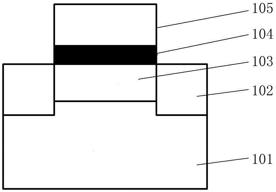
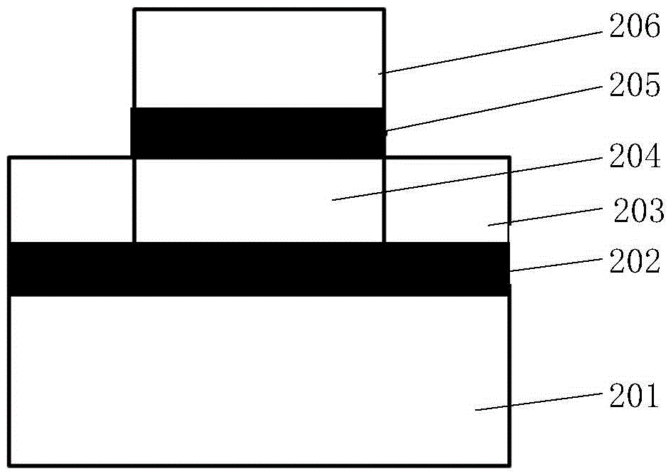
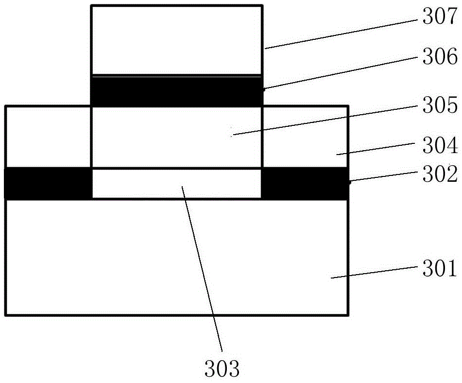
[0032] The fin field effect transistor of the present invention includes a silicon substrate, a fin structure on the silicon substrate, a gate insulating layer and a gate electrode on the fin structure; wherein, the middle part of the fin structure below the gate electrode It is a double-layer structure, which constitutes a double-layer channel structure; the double-layer channel structure includes an upper channel and a lower channel; both ends of the fin structure are single-layer structures, and the single-layer structure and the silicon substrate There is an in...


PUM


Abstract

The invention provides a finned-type field effect transistor structure and a fabrication method thereof. The finned-type field effect transistor structure comprises a silicon substrate, a finned structure, a gate insulation layer and a gate electrode, wherein the fined structure is arranged on the silicon structure, the gate insulation layer and the gate electrode are arranged on the finned structure, a dual-layer structure is arranged at the middle part of the finned structure below the gate electrode and forms a dual-layer channel structure, an upper channel is arranged at the upper layer of the dual-layer structure, a low channel is arranged at the lower layer of the dual-layer structure, single-layer structures are arranged at the two ends of the finned structure, insulation mediums are arranged between the single-layer structures and the silicon substrate, and the single-layer structures form source-drain extension regions. By isolating the source-drain extension regions from the silicon substrate through the insulation mediums, leakage passages between a source and a drain of the device and between devices are effectively blocked, the leakage current is reduced, and the latch-up effect is effectively avoided; on the other hand, the upper channel and the substrate are connected by a semiconductor material of the lower channel, the cooling performance is high, and the self heating effect is prevented; and moreover, the method provided by the invention is low in cost, and the process is simple and controllable.

Description

technical field [0001] The invention relates to the technical field of semiconductors, in particular to a fin field effect transistor and a preparation method thereof. Background technique [0002] For more than half a century, the rapid development of the integrated circuit industry has provided hardware guarantee for the information age. MOS devices are important components in the field of integrated circuits. In 1925, J. Lilienfield proposed the basic principles behind field effect transistors. In 1948, the first field effect transistor was born in the laboratory. Scaling down of devices has been going on throughout the history of integrated circuits because of the benefits of higher on-state current, higher speed, and smaller area that smaller-sized devices can bring. [0003] However, when the feature size of traditional MOS devices is reduced to the nanometer scale, various negative effects begin to emerge. Among them, since the equivalent gate oxide thickness canno...

Claims


Application Information

Patent Timeline
Patent Type & Authority Applications(China)
IPC IPC(8): H01L29/78H01L29/06H01L29/10H01L21/336
CPCH01L29/7851H01L29/0653H01L29/1033H01L29/66795
Inventor 范春晖王全
Owner SHANGHAI INTEGRATED CIRCUIT RES & DEV CENT
Why Eureka
Try Eureka