Semiconductor device with super-junction structure and preparation method thereof

A semiconductor and device technology, which is applied in the field of semiconductor devices with super junction structure and its preparation, can solve the problems of increased switching loss of semiconductor devices, reduced durability of semiconductor devices, and high breakdown voltage of cell regions, so as to reduce the switching Loss, reduce loss and voltage oscillation, optimize the effect of breakdown position

Active Publication Date: 2016-05-11
CHINA RESOURCES MICROELECTRONICS (CHONGQING) CO LTD
View PDF4 Cites 1 Cited by
  • Summary
  • Abstract
  • Description
  • Claims
  • Application Information

AI Technical Summary

Problems solved by technology

[0009] In view of the above-mentioned shortcomings of the prior art, the object of the present invention is to provide a semiconductor device with a super junction structure, which is used to solve the problem in the prior art that due to the second conductivity type guide pillars in the cell region passing through the second conductivity The type of body region is directly connected to the source electrode, which causes the capacitance between the source and the dra...

Method used


Image

  • Semiconductor device with super-junction structure and preparation method thereof
  • Semiconductor device with super-junction structure and preparation method thereof
  • Semiconductor device with super-junction structure and preparation method thereof

Examples


Embodiment 1

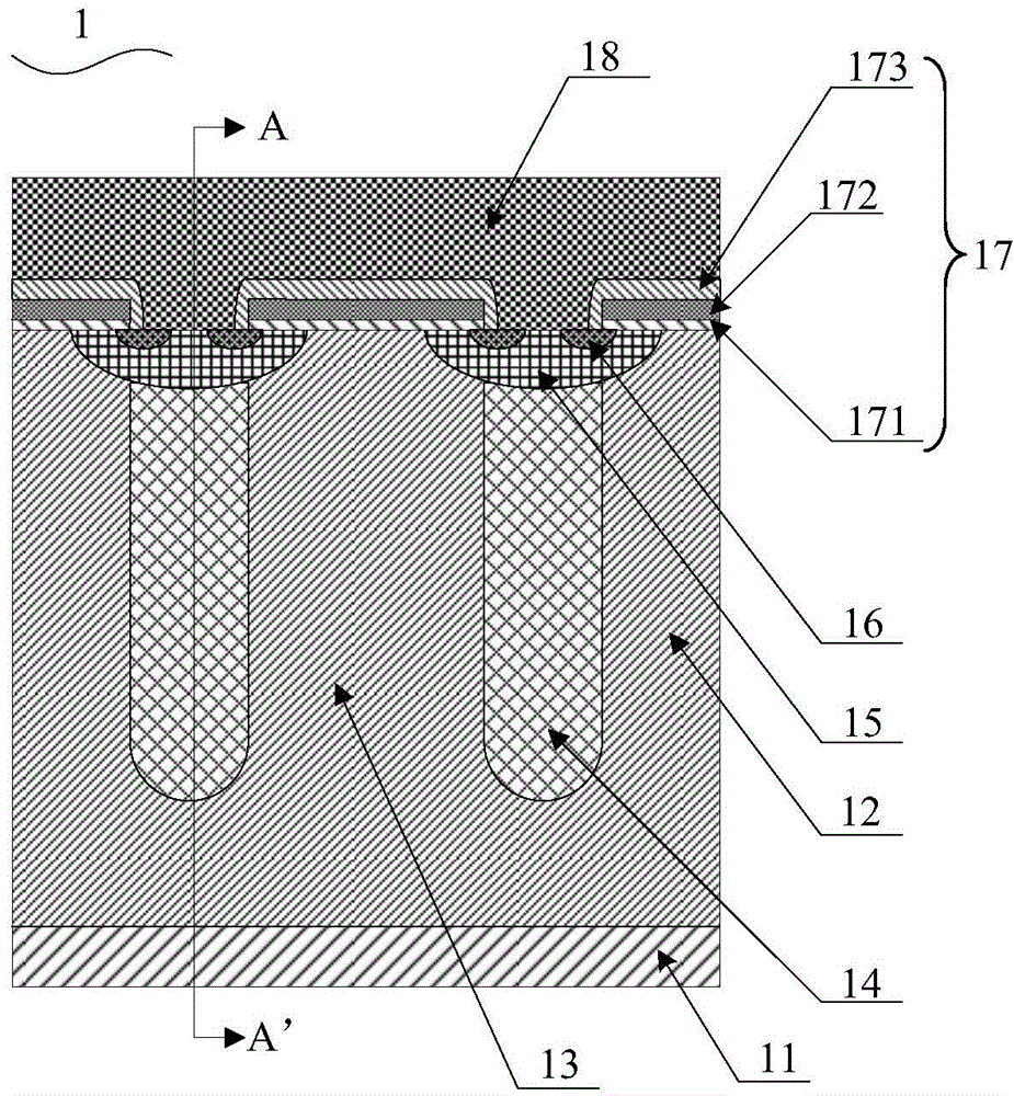
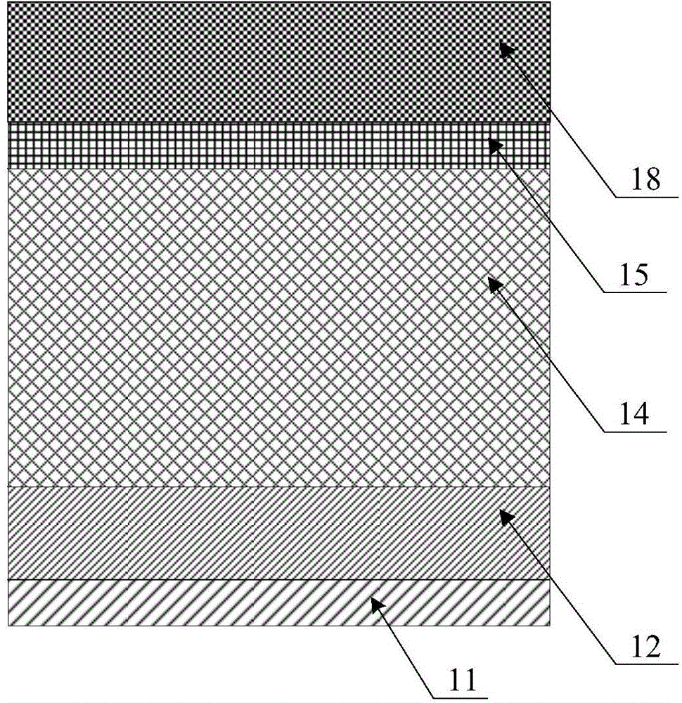
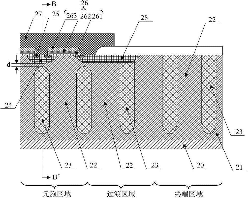
[0080] see Figure 2 to Figure 7 , the present invention provides a semiconductor device with a superjunction structure, the semiconductor device at least includes: a cell region; each of the cell regions includes a substrate 20, a first conductivity type on the substrate 20 The epitaxial layer 21, the guide post 22 of the first conductivity type and the guide post 23 of the second conductivity type located in the epitaxial layer 21 of the first conductivity type; the guide post 22 of the first conductivity type and the guide post 23 of the second conductivity type The guide pillars 23 extend in the epitaxial layer 21 of the first conductivity type along the direction of the current path, and are alternately connected and arranged in the direction perpendicular to the current path to form a super junction structure; the epitaxial layer 21 of the first conductivity type It also includes a first body region 24 of the second conductivity type and a source region 25 of the first c...

Embodiment 2

[0109] see Figure 8 to Figure 11, in this embodiment, a semiconductor device with a super junction structure is also provided, the semiconductor device at least includes: a cell region; the cell region includes a substrate 20, a first substrate located on the substrate 20 The epitaxial layer 21 of the conductivity type, the guide post 22 of the first conductivity type and the guide post 23 of the second conductivity type located in the epitaxial layer 21 of the first conductivity type; the guide post 22 of the first conductivity type and the guide post 23 of the second conductivity type Guide pillars 23 of two conductivity types extend in the epitaxial layer 21 of the first conductivity type along the direction of the current path, and are alternately connected and arranged in the direction perpendicular to the current path to form a super junction structure; The epitaxial layer 21 also includes a first body region 24 of the second conductivity type and a source region 25 of ...

Embodiment 3

[0125] see Figure 12 to Figure 13 , this embodiment also provides a semiconductor device with a super junction structure, the semiconductor device at least includes: a cell region; the cell region includes a substrate 20, a first conductive layer located on the substrate 20 epitaxial layer 21 of the first conductivity type, a guide post 22 of the first conductivity type and a guide post 23 of the second conductivity type located in the epitaxial layer 21 of the first conductivity type; the guide post 22 of the first conductivity type and the second Guide pillars 23 of conductivity type extend in the epitaxial layer 21 of the first conductivity type along the direction of the current path, and are alternately connected and arranged in the direction perpendicular to the current path to form a super junction structure; the epitaxial layers of the first conductivity type Layer 21 also includes a first body region 24 of the second conductivity type and a source region 28 of the fi...


PUM


Abstract

The invention provides a semiconductor device with a super-junction structure. The semiconductor device comprises a cellular area. The cellular area comprises a second-conductive-type first body area, first-conductive-type guide pillars and second-conductive-type guide pillars. A preset distance is kept between each second-conductive-type guide pillar and the first body area above the second-conductive-type guide pillars. The second-conductive-type guide pillars are partially or totally separated from the first body area above the second-conductive-type guide pillars. Capacitance between a source electrode and a drain electrode can be effectively reduced, and furthermore switching loss of the semiconductor device is reduced. The semiconductor device further has functions of restraining minority-carrier injection, restraining minority-carrier extraction in a reverse recovery period, improving a reverse recovery characteristic and reducing loss and voltage oscillation in a reverse recovery period. Through controlling the connecting area between the second-conductive-type guide pillars in the cellular area and the first body area above the second-conductive-type guide pillars, semiconductor device breakdown in the cellular area can be ensured, and furthermore durability of the semiconductor device can be improved.

Description

technical field [0001] The invention belongs to the manufacturing field of semiconductor devices, and relates to a semiconductor device with a super junction structure and a preparation method thereof. Background technique [0002] Metal-Oxide-Semiconductor-Field-Effect Transistor, referred to as Metal-Oxide-Semiconductor Field-Effect Transistor (MOSFET), is a field-effect transistor (field-effect transistor) that can be widely used in analog circuits and digital circuits. . MOSFETs can be divided into N-type and P-type MOSFETs according to the polarity of their "channels", commonly known as NMOSFETs and PMOSFETs. A common N-type MOSFET uses a P-type silicon semiconductor material as the substrate, diffuses it to form an N-type region, covers the top surface with an insulating layer, and finally sets holes on the N-type region as electrodes. In order to improve the characteristics of certain parameters, such as increasing the operating current, increasing the operating vol...

Claims


Application Information

Patent Timeline
IPC IPC(8): H01L29/78H01L29/06H01L21/336
Inventor 马荣耀克里斯坦·皮尔斯
Owner CHINA RESOURCES MICROELECTRONICS (CHONGQING) CO LTD
Why Eureka
Try Eureka