Manufacturing method of transistor

A manufacturing method and technology for transistors, which are used in semiconductor/solid-state device manufacturing, electrical components, circuits, etc., can solve problems such as transistor failure and low yield, and achieve the effects of reducing thickness, reducing losses, and improving controllability

Active Publication Date: 2016-05-18
SEMICON MFG INT (SHANGHAI) CORP
View PDF6 Cites 6 Cited by
  • Summary
  • Abstract
  • Description
  • Claims
  • Application Information

AI Technical Summary

Problems solved by technology

[0008] However, when testing the transistors formed by the above process,

Method used


Image

  • Manufacturing method of transistor
  • Manufacturing method of transistor
  • Manufacturing method of transistor

Examples


Example Embodiment

[0037] It can be known from the background technology that the transistors formed in the prior art are prone to failure and low yield.
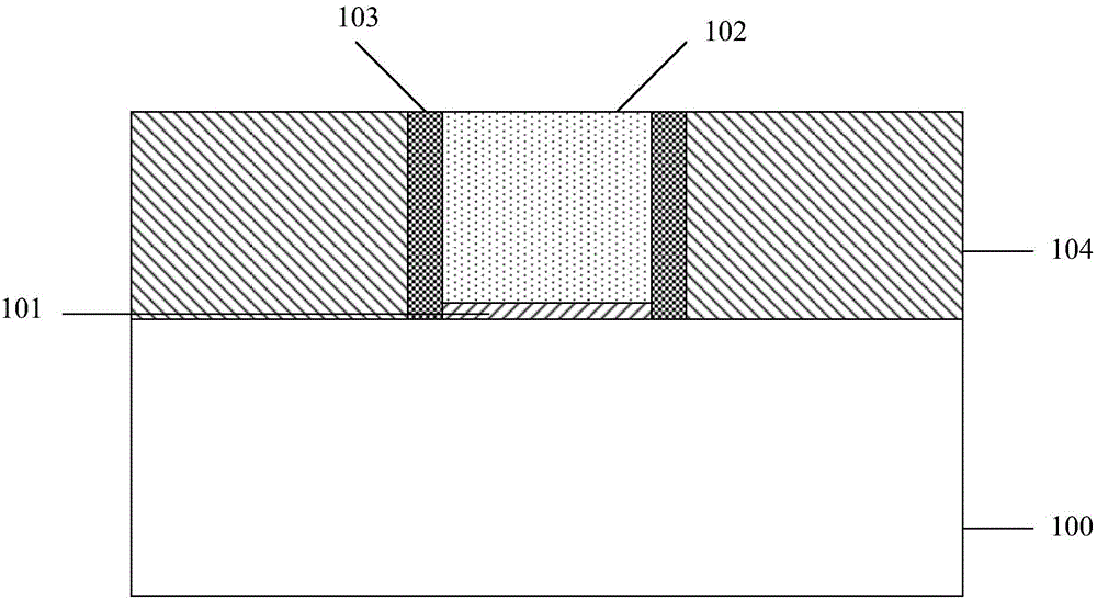
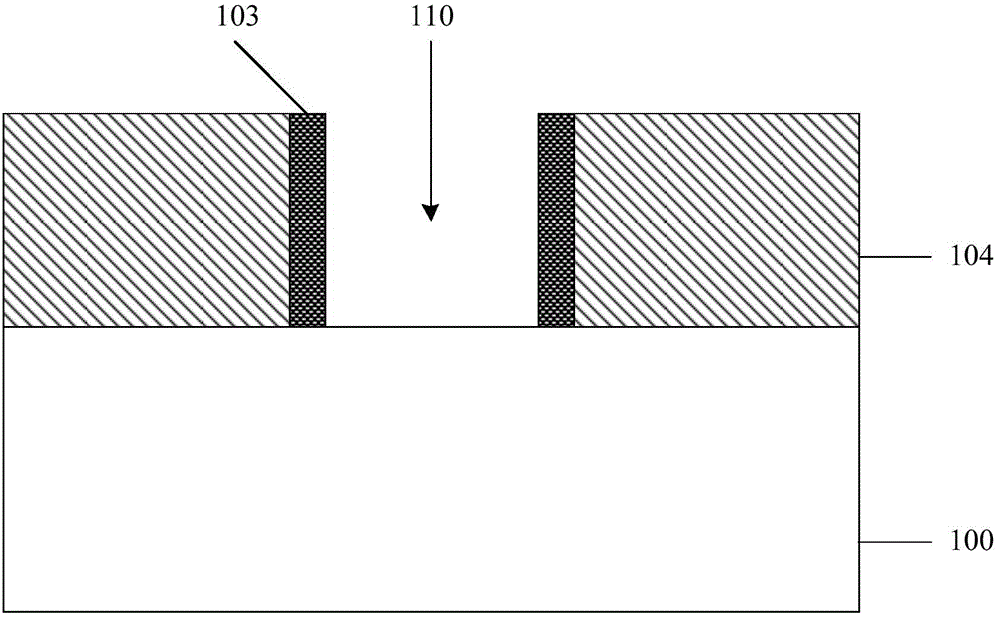
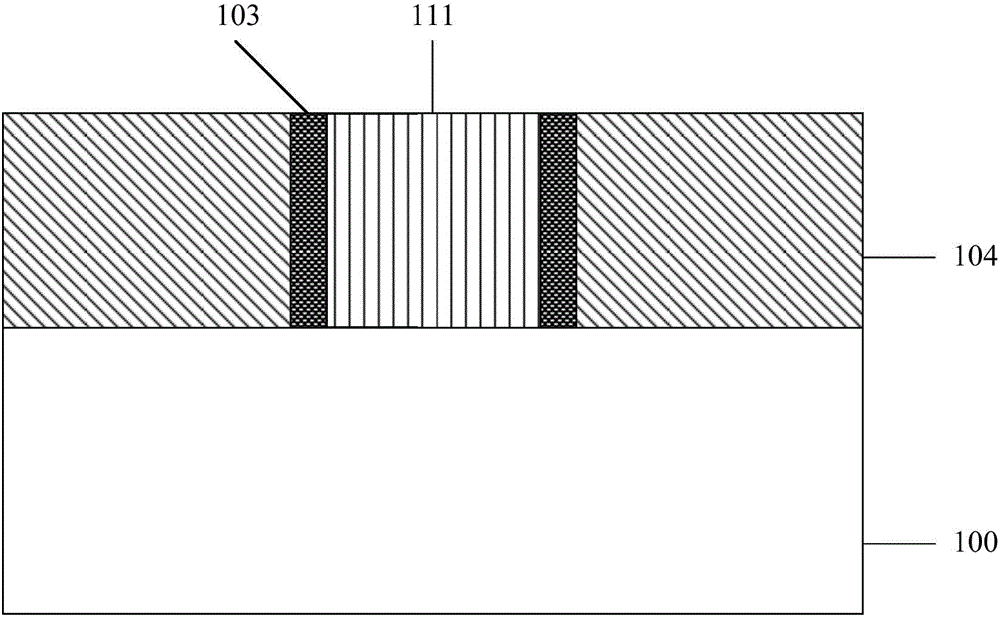
[0038] Combine Figure 1 to Figure 3 The schematic diagram of the manufacturing method of the prior art transistor is shown, and the reasons for transistor failure and low yield are analyzed:

[0039] reference figure 1 The material of the transistor protective layer 101 and the material of the interlayer dielectric layer 104 are the same oxides. When the protective layer 101 is cleaned and removed by a diluted hydrofluoric acid solution, a part of the thickness of the interlayer dielectric layer 104 is also consumed. Moreover, due to the different formation processes of the protective layer 101 and the interlayer dielectric layer 104 (the method for forming the protective layer 101 is mostly a thermal oxidation process, and the method for forming the interlayer dielectric layer 104 is mostly a chemical vapor deposition process), diluted hydrofluor...


PUM


Abstract

The invention discloses a manufacturing method of a transistor. The method comprises the following steps: providing a semiconductor substrate; successively forming a protective layer, an etching barrier layer and a pseudo grid material layer on the semiconductor substrate; performing first etching on the protective layer, the etching barrier layer and the pseudo grid material layer to form pseudo grids, and a residual etching barrier layer and a residual protection layer which are disposed below the pseudo grids; forming an interlayer dielectric layer on the semiconductor substrate between the pseudo grids; removing the pseudo grids to form a groove exposing the residual etching barrier layer; removing the residual etching barrier layer and the residual protection layer which are disposed in the groove to expose the substrate; and filling the groove exposing the substrate with a grid dielectric layer and a metal material to form a metal grid electrode. According to the invention, through additionally arranging the etching barrier layer on the protective layer, etching with the pseudo grids removed is enabled to well stop at the etching barrier layer, such that the requirements of pseudo grid structure etching and interlayer dielectric layer loss for the thickness of the protective layer are balanced, the performance of the formed transistor is improved, and the yield of the formed transistor is improved.

Description

technical field [0001] The invention relates to the field of manufacturing semiconductor devices, in particular to a method for manufacturing a transistor. Background technique [0002] With the continuous development of integrated circuit manufacturing technology, the feature size of MOS transistors is getting smaller and smaller. In order to reduce the parasitic capacitance of the gate of MOS transistors and improve the device speed, the gate structure of high-K gate dielectric layer and metal gate is adopted. introduced into the MOS transistor. [0003] The "Gate-Last" process is widely used in the manufacturing process of high-K gate dielectric layer and metal gate. Compared with the "Gate-First" process, the devices fabricated by the Gate-Last process can avoid the influence of the annealing of the source region or the drain region on other structures of the transistor. Therefore, the stability of devices fabricated by the gate-last process is higher. [0004] refer ...

Claims


Application Information

Patent Timeline
IPC IPC(8): H01L21/336
Inventor 毛刚叶好华
Owner SEMICON MFG INT (SHANGHAI) CORP
Why Eureka
Try Eureka