OLED display panel and manufacturing method thereof

A technology of a display panel and a manufacturing method, applied in the field of OLED display panels, can solve the problems of disadvantageous large-size AMOLED, reduce the luminous efficiency of blue light devices, affect the transmittance, etc. The effect of coverage reduction

Inactive Publication Date: 2016-05-18
KUNSHAN GO VISIONOX OPTO ELECTRONICS CO LTD
View PDF4 Cites 45 Cited by
  • Summary
  • Abstract
  • Description
  • Claims
  • Application Information

AI Technical Summary

Problems solved by technology

However, in top-emitting OLED panels, the cathode is usually made of metals such as Mg and Ag. In order to ensure the light output rate, the cathode requires high light transmittance, so the cathode is generally relatively thin. The thickness of the cathode of the top-emitting OLED panel is usually only When the cathode is thinner, the resistance is too high, which will cause IR voltage drop (that is, the voltage drop caused by the resistance of the cathode), which is not conducive to the production of large-scale AMOLED; and when the thickness of the cathode is thicker, it will affect the transmittance, especially reduce the blue light. Device Luminous Efficiency

Method used


Image

  • OLED display panel and manufacturing method thereof
  • OLED display panel and manufacturing method thereof
  • OLED display panel and manufacturing method thereof

Examples


Embodiment Construction

[0041] In order to further explain the technical means and effects of the present invention to achieve the intended purpose of the invention, the specific implementation, structure, features and effects of the present invention will be described in detail below in conjunction with the accompanying drawings and examples.

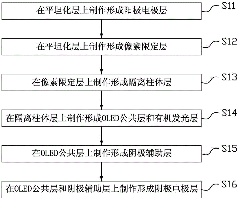
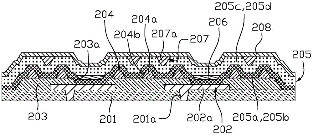
[0042] An embodiment of the present invention provides a method for manufacturing an OLED display panel, please refer to Figure 2 to Figure 3 , the production method includes the following steps:

[0043] S11: forming an anode electrode layer 202 on the planarization layer 201;

[0044] In step S11, an anode electrode layer 202 is formed on the upper surface of the planarization layer 201. Specifically, a layer of conductive material can be deposited on the planarization layer 201 by methods such as magnetron sputtering, and then the conductive material layer can be deposited on the planarization layer 201 by a photolithography process. The material layer i...


PUM


Abstract

The invention provides an OLED (Organic Light-Emitting Diode) display panel and a manufacturing method thereof. The OLED display panel comprises an anode electrode layer formed on a planarization layer, a pixel limitation layer formed on the planarization layer and located on the periphery of each sub-pixel, an isolated cylinder layer formed on the pixel limitation layer, an OLED public layer formed on the isolated cylinder layer, a cathode auxiliary layer formed on the OLED public layer and a cathode electrode layer formed on the OLED public layer and electrically connected to the cathode auxiliary layer. The anode electrode layer comprises a plurality of anode electrodes mutually isolated; each anode electrode corresponds to a sub-pixel. The isolated cylinder layer comprises a plurality of isolated cylinders mutually isolated, and the isolated cylinders are formed on the upper surface of the pixel limitation layer and located between adjacent sub-pixels; at least two isolated cylinders are arranged between adjacent sub-pixels, and a groove is formed between adjacent isolated cylinders. The cathode auxiliary layer comprises a plurality of auxiliary bus bars which are embedded into the OLED public layer, and respectively correspond to grooves arranged between adjacent isolated cylinders.

Description

technical field [0001] The invention relates to the technical field of OLED display panels, in particular to an OLED display panel and a manufacturing method thereof. Background technique [0002] Organic light-emitting diode OLED (Organic Light-Emitting Diode) is an active light-emitting device, which has the characteristics of high contrast, wide viewing angle, low power consumption, fast response, thinner volume and flexibility. It has received more and more attention and is expected to become The next-generation mainstream flat-panel display technology is one of the most concerned technologies among flat-panel display technologies. [0003] Active Matrix Organic Lighting Emitting Display (AMOLED) uses thin-film transistors (TFTs) with capacitors to store signals to control the brightness and grayscale performance of OLED pixels. AMOLED has the characteristics of large size, relatively low power consumption, high resolution, and long panel life, so it has been highly val...

Claims


Application Information

Patent Timeline
Patent Type & Authority Applications(China)
IPC IPC(8): H01L27/32H01L51/52H01L51/56
CPCH10K59/122H10K50/824H10K71/00
Inventor 李振伟陈红
Owner KUNSHAN GO VISIONOX OPTO ELECTRONICS CO LTD
Why Eureka
Try Eureka