Preparation method of ZnO transparent conductive film

A transparent conductive thin film and thin film technology, applied in the direction of solid-state chemical plating, metal material coating process, coating, etc., can solve the problems of high preparation cost, unfriendly environment, limited use, etc., and achieve simple operation and simple regulation , Regulate the practical effect

Inactive Publication Date: 2016-05-25
SHENZHEN GUOHUA OPTOELECTRONICS +1
View PDF7 Cites 2 Cited by
  • Summary
  • Abstract
  • Description
  • Claims
  • Application Information

AI Technical Summary

Problems solved by technology

[0005] The purpose of the present invention is to provide a preparation method for ZnO transparent conductive film, aiming to solve the problems that the transparent conductive film in the prior art is ITO, which has high preparation cost, limited use and unfriendly environment

Method used


Image

  • Preparation method of ZnO transparent conductive film
  • Preparation method of ZnO transparent conductive film
  • Preparation method of ZnO transparent conductive film

Examples


Embodiment 1

[0020] The preparation method of the ZnO transparent conductive film provided in this embodiment comprises the following preparation steps:

[0021] a), with Zn(Ac) 2 2H 2 O, Al(NO 3 ) 3 9H2O, FeCl 3 ·6H 2 O is a raw material, ethylene glycol methyl ether is a solvent, and ethanolamine is a stabilizer, which is configured into a sol in a certain proportion;

[0022] b), cleaning the glass substrate;

[0023] c) Spin-coat the sol obtained in step a) on the cleaned glass substrate in step b) to form a film; place the coated glass substrate in an oven at 150°C to 250°C for heat treatment for 9 minutes to After 11 minutes, take it out, cool it down to room temperature naturally, and then repeat the spin-coating sol several times to form a film;

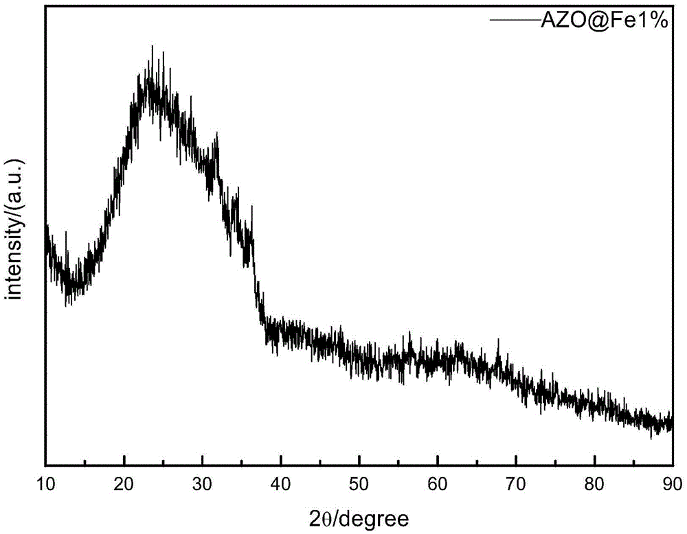
[0024] d) heat-treating the thin film prepared in step c) in the air environment, then a ZnO transparent conductive thin film with high transmittance in the visible light band can be obtained.

[0025] In the above-mentioned prepa...

Embodiment 2

[0033] The difference between this embodiment and Embodiment 1 is:

[0034] In this embodiment, in step a), with Zn(Ac) 2 2H 2 O, Al(NO 3 ) 3 9H2O, FeCl 3 ·6H 2 O and CoCl2·6H2O are raw materials, among which, the concentration of Co ions is 0.005mol / L~0.035mol / L, and the total concentration of Fe ions and Co ions is kept in the range of 0.01~0.07mol / L, and other preparation conditions remain unchanged .

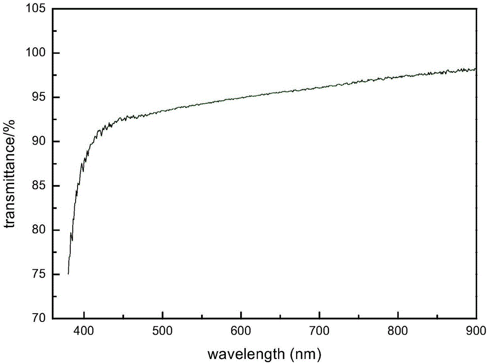
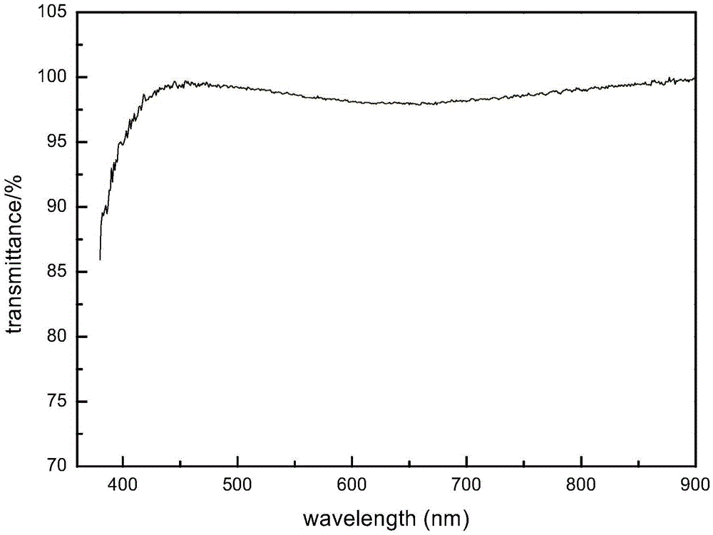
[0035] refer to image 3 As shown, the ZnO transparent conductive film has a transmittance of over 90% in the visible light band.

Embodiment 3

[0037] The difference between this embodiment and embodiment two is:

[0038] In step c), the spin coating is repeated seven times on the glass substrate to obtain a thicker ZnO transparent conductive film.


PUM


Abstract

The invention relates to the technical field of transparent conductive films and discloses a preparation method of a ZnO transparent conductive film. The preparation method includes the steps of a, using Zn(Ac)2.2H2O, Al(NO3)3.9H2O and FeCl3.6H2O as raw materials, ethylene glycol monomethyl ether as solvent, ethanolamine as stabilizer to prepare sol; b, cleaning a glass substrate; c, using a spin-coating method to form a film on the glass substrate; heating in a drying oven of 150-250 DEG C for 9-11 minutes, naturally cooling to room temperature, and repeatedly spin coating the sol for multiple times to form a film; d, performing thermal treatment on the film obtained in the step c to obtain the ZnO transparent conductive film. The preparation method using a sol-gel method to synthesize the ZnO transparent conductive film has the advantages that the method is simple to operate, economical and convenient, capable of achieving large-scale production, and the like, and the prepared ZnO transparent conductive film is uniform.

Description

technical field [0001] The invention relates to the technical field of transparent conductive films, in particular to a preparation method of ZnO transparent conductive films. Background technique [0002] ZnO is a direct bandgap II-VI compound semiconductor with a wide bandgap (3.3eV at room temperature). The exciton binding energy of ZnO is 60meV and has a hexagonal wurtzite structure. ZnO thin film has good light transmittance, piezoelectricity, photoelectricity, gas sensitivity and pressure sensitivity, and is easy to realize integration with various semiconductor materials. Based on these excellent properties, ZnO has a wide range of practical applications in many fields, such as transparent electrodes, ultraviolet light-emitting devices, transistors, chemical sensors, gas sensors, and solar cells. At the same time, using different dopants and changing the doping level of the dopant can effectively change the electrical and optical properties of ZnO, so as to meet the ...

Claims


Application Information

Patent Timeline
IPC IPC(8): C23C20/08
CPCC23C20/08
Inventor 李楠李旦水玲玲金名亮周国富
Owner SHENZHEN GUOHUA OPTOELECTRONICS
Why Eureka
Try Eureka