Wafer level package method for reducing edge stress

A wafer-level packaging, edge stress technology, used in electrical components, semiconductor/solid-state device manufacturing, circuits, etc., can solve problems such as cracking, delamination, affecting the reliability of metal wiring layers, and achieve improved electrical connection, increase The effect of package reliability

Inactive Publication Date: 2016-06-01
BEIJING UNIV OF TECH
View PDF4 Cites 8 Cited by
  • Summary
  • Abstract
  • Description
  • Claims
  • Application Information

AI Technical Summary

Problems solved by technology

[0003] At present, after the wafer is cut, the interface between the dielectric layer on the edge of the chip and the supporting wall is in the process of reliability testing (such as TC, HAST, etc.), and due to the concentrated stress, failures such as delamination and cracking are prone to occur phenomenon, which will also seriously affect the reliability of the metal wiring layer in the package

Method used


Image

  • Wafer level package method for reducing edge stress
  • Wafer level package method for reducing edge stress
  • Wafer level package method for reducing edge stress

Examples


Embodiment Construction

[0046] The present invention will be described in more detail below with reference to accompanying drawing:

[0047] The wafer-level packaging manufacturing process for reducing edge stress of this embodiment will be described in detail below with reference to FIGS. (1) to (8).

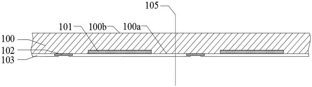
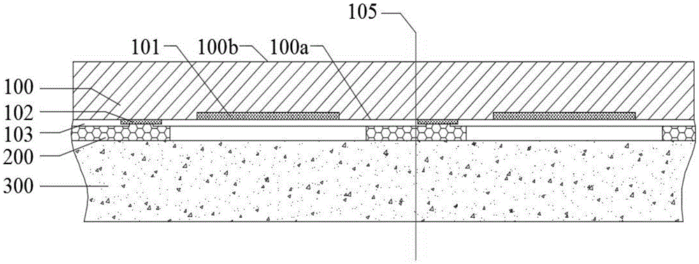
[0048] Step 1, provide wafer 100:

[0049] Referring to FIG. (1), a wafer 100 is provided, and a functional area 101 , pads 102 , and a dielectric layer 103 are formed on the wafer 100 . The functional areas, pads, and dielectric layers are formed on the wafer 100 . In other embodiments, the wafer material may be semiconductor materials such as germanium and gallium arsenide.

[0050] There is a dicing line 105 with a certain width between adjacent functional areas 101 of the wafer, and the dicing line does not cover the pad. Dicing along this scribe line separates the wafer into individual chips.

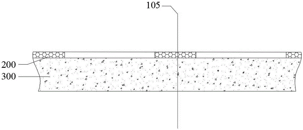
[0051] Step 2, bonding the cover plate 300 and the support wall 200:

[0052] Referring to Figure ...


PUM


Abstract

The invention relates to the field of wafer level chip package, and relates to a wafer level package method for reducing edge stress. The method comprises the following steps of 1, providing a wafer with a functional region and a bonding pad; 2, providing a cover plate, wherein the cover plate is bonded with a support wall; 3, bonding the cover plate with the support wall with the wafer by a bonding adhesive; 4, pre-cutting the position of a cutting channel on a second surface of the wafer, and cutting and removing a certain thickness of the support wall to form a first groove body; 5, etching the second surface of the wafer, removing a material on the bonding pad to form a second groove body; 6, making a redistribution layer, in which the redistribution layer is made on the second surface of the wafer; and 7, cutting the wafer along the cutting channel to form package of a single chip. By wrapping and protecting the edge of the cutting channel, a metal layer and a dielectric layer, the risk that a part of the chip edge is layered and cracked is reduced, and electrical connection between the bonding pad and a metal line is improved.

Description

technical field [0001] The invention relates to the field of wafer-level chip packaging, in particular to a wafer-level packaging method for reducing edge stress. Background technique [0002] The general structure of the wafer includes several chip units, each chip unit includes a substrate and a dielectric layer located on the front side of the substrate, the front side of the substrate is provided with a functional area, and several pads are provided around the functional area, and the pads Located in the dielectric layer, the functional area is electrically connected to the surrounding pads. At present, the interconnection steps of wafer-level chips include making an opening on the back of the wafer substrate, the opening extends from the back of the wafer to the front of the wafer, and exposes the pads on the front, and laying metal lines on the inner wall of the opening , lead the electrical properties of the pad to the back of the wafer to realize the interconnection...

Claims


Application Information

Patent Timeline
Patent Type & Authority Applications(China)
IPC IPC(8): H01L21/304H01L21/78
CPCH01L21/304H01L21/78
Inventor 秦飞史戈别晓锐安彤肖智轶
Owner BEIJING UNIV OF TECH
Why Eureka
Try Eureka