Cu2-xS self-doped semiconductor optothermal material and application thereof to invisible fingerprint imaging

An invisible fingerprint, cu2-xs technology, used in nanotechnology, application, medical science and other directions for materials and surface science, can solve the problem that hydrophobic nanoparticles are not suitable for binding fingerprints, and have not been used in invisible fingerprint photothermal imaging, etc. problem, to achieve the effect of eliminating interference

Active Publication Date: 2016-06-15
BEIJING UNIV OF CHEM TECH
View PDF7 Cites 3 Cited by
  • Summary
  • Abstract
  • Description
  • Claims
  • Application Information

AI Technical Summary

Problems solved by technology

Explore Cu-based 2-x The application of S self-doped semiconductor photothermal materials in photothermal imaging has aroused great interest, but this material has not been used in photothermal imaging of invisible fingerprints, mainly because of the hydrophobic Non-toxic nanoparticles are not good for binding fingerprints

Method used


Image

  • Cu2-xS self-doped semiconductor optothermal material and application thereof to invisible fingerprint imaging
  • Cu2-xS self-doped semiconductor optothermal material and application thereof to invisible fingerprint imaging
  • Cu2-xS self-doped semiconductor optothermal material and application thereof to invisible fingerprint imaging

Examples


Embodiment 1

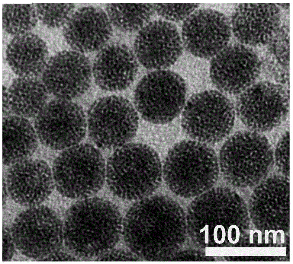
[0015] a. Take Cu dispersed in chloroform 2-x S nanoparticles, x = 0.25, where Cu 2-x The content of S nanoparticles is 9.6mg, mixed with 4.5mg allyl thiol and dispersed in 1mL chloroform, after stirring for 30min, add 70μLAIBN (0.5mg / mL); then add 10mL SDS aqueous solution (1.8mg / mL), ice bath After ultrasonication for 3min, irradiate with 365nm light for 10min and stir overnight at room temperature, after centrifugal purification, disperse in 2mL ultrapure water to obtain Cu-based 2-x S self-doping semiconductor photothermal material dispersion;

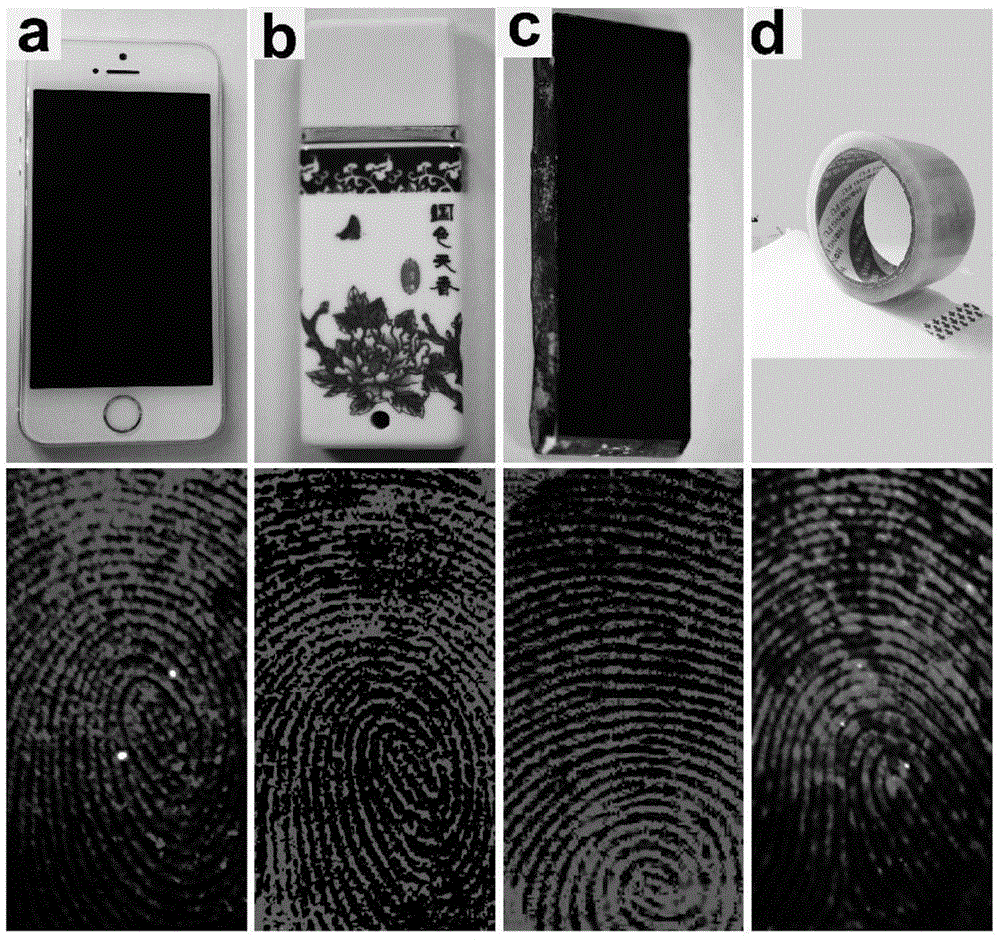
[0016] b. After aging the fingerprint sample at 30°C for 48 hours, add 200 μL of the Cu-based 2-x S self-doped semiconductor photothermal material dispersion, incubate at room temperature for 3 minutes and remove excess liquid.

[0017] c. Under near-infrared light irradiation, with the help of a near-infrared imager, the imaging of invisible fingerprints is realized.

Embodiment 2

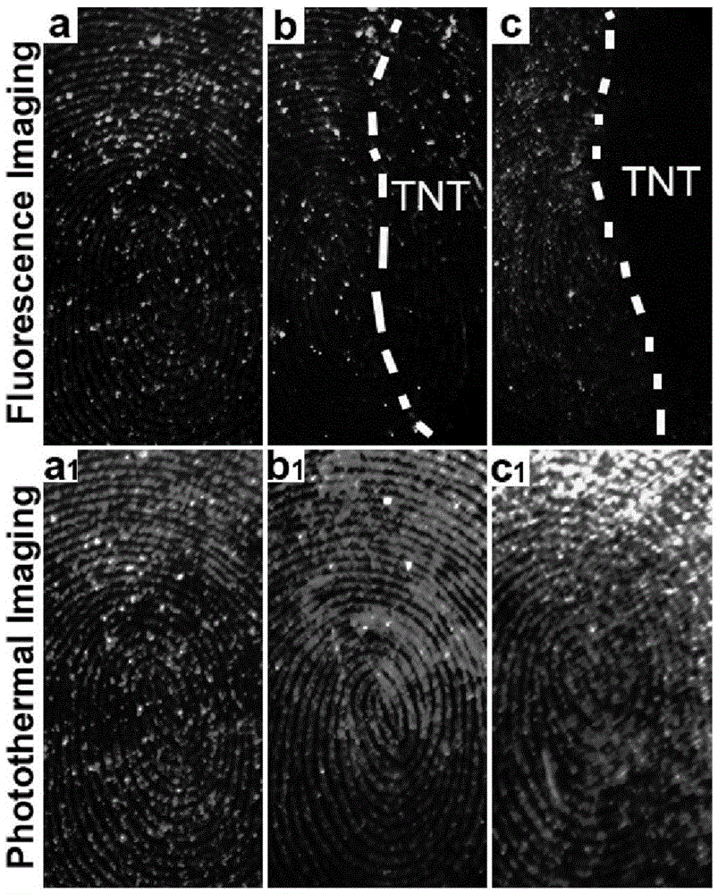
[0019] Based on the Cu that step b adds among the embodiment 1 2-x S self-doping semiconductor photothermal material dispersion was replaced by Cu with a volume ratio of 1:1 2-x Mixed solution obtained from S self-doped semiconductor photothermal material dispersion and CdSeZnS quantum dot dispersion, Cu 2-x The mass ratio of S self-doping semiconductor photothermal material to CdSeZnS quantum dots is 1:1, which can realize the imaging of invisible fingerprints containing 2,4,6-trinitrotoluene explosive residues.


PUM


Abstract

The invention discloses a Cu2-xS self-doped semiconductor optothermal material and application thereof to invisible fingerprint imaging. As polymerization of allyl thiol is used for modifying the surface of the Cu2-xS self-doped semiconductor material with high photothermal conversion efficiency, the Cu2-xS self-doped semiconductor material has amphipathy and can be selectively adsorbed to an invisible fingerprint, and the invisible fingerprint can be imaged clearly under the complicated background by means of near-infrared light radiation and near-infrared imager. In addition, a fluorescence-optothermal bimodal imaging method realized by the Cu2-xS-CdS3@ZnS nanocomposite material is used, residues of 2,4,6-trinitrotoluene and other powerful explosive materials contained in the invisible fingerprint are detected successfully on the condition that fingerprint morphology imaging is complete, a powerful means is provided for scouting crime evidence of criminal offenders, and the Cu2-xS self-doped semiconductor optothermal material can play an important role in judicial expertise and anti-terrorist application.

Description

technical field [0001] The invention belongs to the technical field of invisible fingerprint imaging, in particular to a Cu-based 2-x S self-doping semiconductor photothermal materials and their applications in invisible fingerprint imaging. Background technique [0002] Since fingerprints are unique marks for each person, the visualization and distinction research of invisible fingerprints has played an important role in forensic identification and anti-terrorism applications. In addition, the secretion of drug metabolites and residues of explosives in fingerprints provides important information for studying the behavior of specific groups of people. To date, methods including electrochemical, optical tomographic coherence imaging, mass spectrometry, infrared, and Raman spectroscopy have been successfully applied to fingerprint imaging and detection of illegal drug and explosive residues in invisible fingerprints, but The main problem these technologies face is that they ...

Claims


Application Information

Patent Timeline
Patent Type & Authority Applications(China)
IPC IPC(8): A61B5/1172B82Y30/00
CPCA61B5/1172B82Y30/00
Inventor 汪乐余崔家斌许苏英
Owner BEIJING UNIV OF CHEM TECH
Why Eureka
Try Eureka