Array substrate and manufacturing method therefor

The technology of an array substrate and its manufacturing method, which is applied in the field of display, can solve the problems of high production cost, achieve the effects of reasonable structure, save photolithography process, and reduce the use of photomasks

Active Publication Date: 2016-06-15
SHENZHEN CHINA STAR OPTOELECTRONICS TECH CO LTD
View PDF3 Cites 11 Cited by
  • Summary
  • Abstract
  • Description
  • Claims
  • Application Information

AI Technical Summary

Problems solved by technology

In the currently commonly used IGZO array substrates, the Etching Stop Layer (ESL, EtchingStopLayer) structure device has better electrical stability than other structures due to the existence of a protective layer, but the IGZO array with an etch stop layer st

Method used


Image

  • Array substrate and manufacturing method therefor
  • Array substrate and manufacturing method therefor
  • Array substrate and manufacturing method therefor

Examples


Embodiment Construction

[0046] In order to further illustrate the technical means adopted by the present invention and its effects, the following describes in detail in conjunction with preferred embodiments of the present invention and accompanying drawings.

[0047] see Figure 1-12 , the present invention provides a method for manufacturing an array substrate, comprising the following steps:

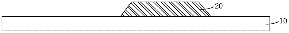
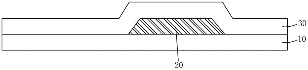
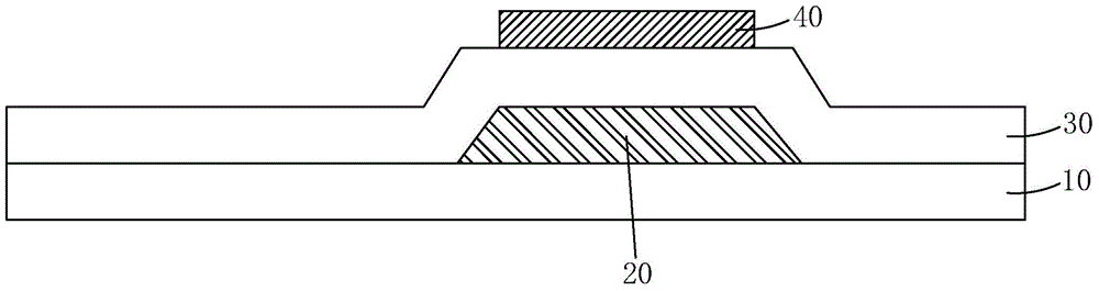
[0048] Step 1, such as figure 1 As shown, a substrate 10 is provided, a first metal layer is formed on the substrate 10 by physical vapor deposition (PVD), and the first metal layer is patterned through a photolithography process to obtain a gate 20 .

[0049] Specifically, the substrate 10 is a transparent substrate, preferably a glass substrate.

[0050] Specifically, the material of the first metal layer may be one or more stacked combinations of molybdenum (Mo), titanium (Ti), aluminum (Al), and copper (Cu).

[0051] Specifically, the photolithography process includes a photolithography process, a wet...


PUM


Abstract

The invention provides an array substrate and a manufacturing method therefor. According to the manufacturing method for the array substrate, a halftone photomask and a one-time photoetching process are adopted to perform patterning processing for a passivation layer and an etching stop layer; a first via hole corresponding to the upward side of a source electrode is formed in the passivation layer; a second via hole and a third via hole positioned between the source electrode and the drain electrode are formed in the etching stop layer; then a pixel electrode connected with the source electrode through the first via hole, a first connecting layer connected with the source electrode and the active layer through the second via hole, and a second connecting layer connected with the drain electrode and the active layer through the third via hole are formed above the passivating layer, the source electrode, the drain electrode and the etching stop layer through the one-time photoetching process. By adoption of the processes, the number of the photoetching processes of an IGZO (indium gallium zinc oxide) array substrate with the etching stop layer structure is reduced; the six times of photoetching process in the prior art are reduced to five times, so that one time of photoetching process is saved, the use of the light-shading cover is reduced, and the production cost of the IGZO array substrate is lowered consequently.

Description

technical field [0001] The present invention relates to the field of display technology, in particular to an array substrate and a manufacturing method thereof. Background technique [0002] With the development of display technology, liquid crystal displays (Liquid Crystal Display, LCD) and other flat display devices are widely used in mobile phones, TVs, personal digital assistants due to their advantages of high image quality, power saving, thin body and wide application range. , digital cameras, notebook computers, desktop computers and other consumer electronics products have become the mainstream of display devices. [0003] Most of the liquid crystal display devices currently on the market are backlight liquid crystal displays, which include a liquid crystal display panel and a backlight module. The working principle of the liquid crystal display panel is to place liquid crystal molecules between two parallel glass substrates. There are many vertical and horizontal s...

Claims


Application Information

Patent Timeline
IPC IPC(8): H01L21/84H01L27/12
CPCH01L27/124H01L27/1288
Inventor 周志超
Owner SHENZHEN CHINA STAR OPTOELECTRONICS TECH CO LTD
Why Eureka
Try Eureka