Large-size light guide plate with lens array and processing method thereof
A lens array and processing method technology, applied in the field of light guide plates, can solve problems such as the inability to directly produce large-size light guide plates, technical limitations of light guide plates, etc., and achieve the effect of preventing smooth forming and accurate mass production
- Summary
- Abstract
- Description
- Claims
- Application Information
AI Technical Summary
Problems solved by technology
Method used
Image
Examples
Embodiment 1
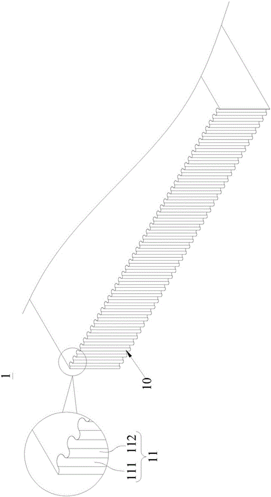
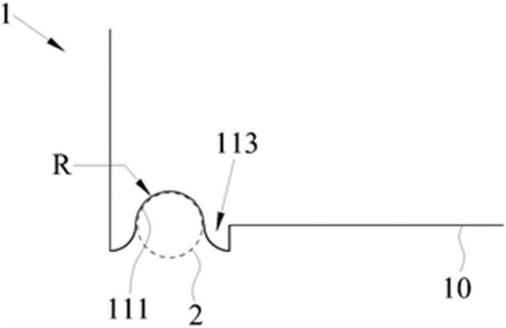
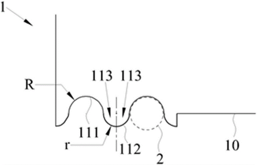
[0054] Since injection molding and tool cutting are currently used in the field of large-size light guide plates, there are many inconveniences for microstructure processing. Therefore, how to quickly mass-produce a large-sized light guide plate with a precise lens array pattern while maintaining the quality of the light guide plate is the technical feature to be revealed by the present invention. see figure 1 , figure 2 and image 3 , which is a three-dimensional structural schematic diagram and various processing schematic diagrams of Embodiment 1 of the present invention, wherein each figure is only for the convenience of explaining the technical features of the present invention. The present invention discloses a large-sized light guide plate 1 with a lens array, including a light-incident surface 10 and a lens array 11 , so that the hot spot phenomenon of the light guide plate 1 can be alleviated through the lens array 11 .
[0055] The light incident surface 10 guides ...
Embodiment 2
[0061] see Figure 4 , Figure 5 and Figure 6 , which is a flow chart of steps and a schematic diagram of each process in Embodiment 2 of the present invention. The present invention also discloses a processing method of a large-sized light guide plate with a lens array, which can quickly mass-produce a large-scale light guide plate and maintain a very high product yield rate. The processing method includes the following steps.
[0062] In step S01 , a plurality of light guide plates 1 stacked in batches are provided, and a light incident surface 10 of each light guide plate 1 is aligned with each other to form a processing plane S. Thus, a plurality of large-sized light guide plates 1 can be processed at one time, and the production rate can be improved.
[0063] Step S02 , bombard the processing plane S with a laser beam 2 to form an arc-shaped groove 111 on each incident surface 10 and generate molten material, and the bombardment condition is defined as the radius of t...
PUM
 Abstract
Description
Claims
Application Information


