Forming process of burr-free printed circuit board (PCB)

A technology of PCB board and forming process, which is applied in the field of burr-free PCB board forming process, which can solve problems affecting process capacity and pass rate, product performance and yield decline, half-hole copper wire residue, etc., so as to avoid material deviation and deformation , Saving process steps and reducing machining paths

Inactive Publication Date: 2016-06-22
PLOTECH TECH KUNSHAN CO LTD
View PDF4 Cites 5 Cited by
  • Summary
  • Abstract
  • Description
  • Claims
  • Application Information

AI Technical Summary

Problems solved by technology

This kind of half hole is formed by cutting the circular plated through hole in half directly after the circular plated through hole is formed. Due to the better ductility of the copper in the hole and the pulling caused by mechanical cutting, if it is not If it is properly handled, it is easy to have half-hole copper wire residue and copper peeling phenomenon, which is the so-called half-hole burr problem, which affects the function of the half-hole, resulting in a decrease in product performance and yield, which in turn increases costs.
[0004] Chinese patent CN101152674 provides a "shape processing method", which provides a good idea to avoid burrs when cutting in half at the machining level. However, this method only reduces the size of burrs, which is still difficult to avoid after the need processing steps to eradicate burrs, which affects process throughput and yield

Method used


Image

  • Forming process of burr-free printed circuit board (PCB)
  • Forming process of burr-free printed circuit board (PCB)
  • Forming process of burr-free printed circuit board (PCB)

Examples


Embodiment 1

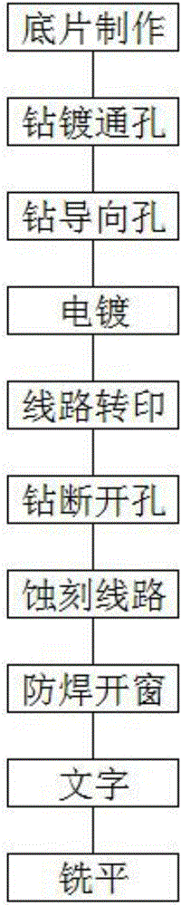
[0045] Such as figure 1 As shown, a burr-free PCB board forming process, the steps include:

[0046] ① Production of film: Carry out CAM design of circuit film and solder mask film according to the original design drawing, in which the line width of the CAM design circuit is 10% wider than the original design drawing, and the diameter of the CAM design welding mask window is 20% larger than the original design drawing. At the same time, the image of the solder mask image designed by CAM compensates for the overlapping part of the line-solder mask that is larger than the range of the pad 42, such as Figure 8 ;

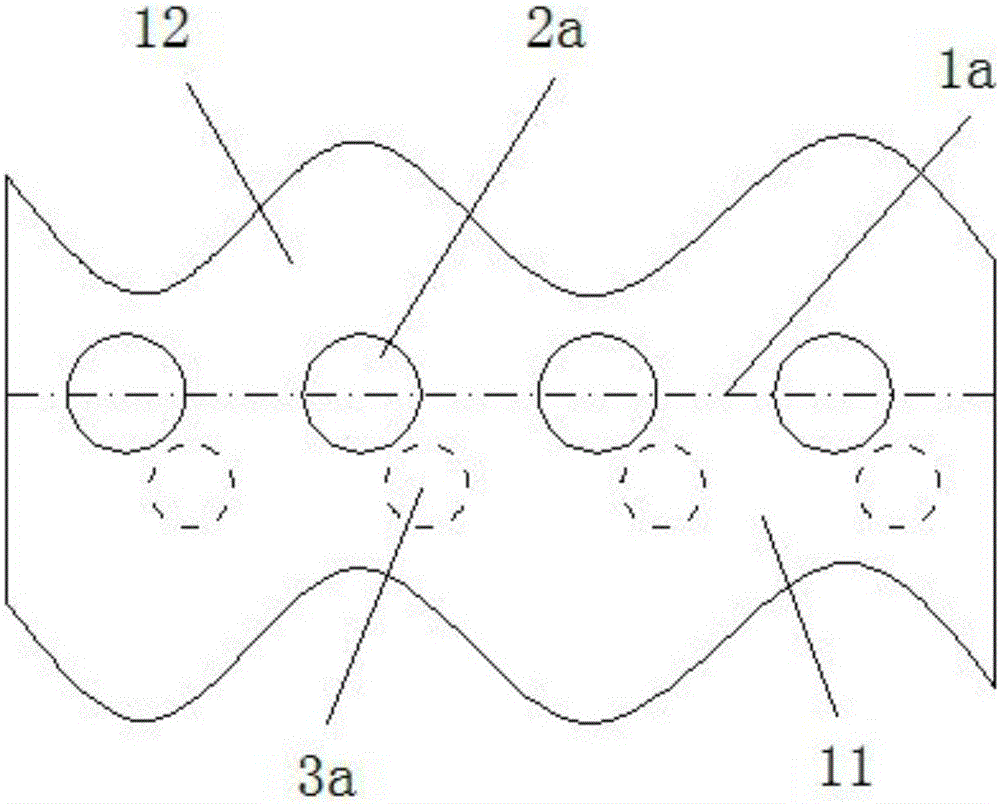
[0047] ②Drilling the plated through hole 2a: drill a plated through hole 2a with a diameter D on the boundary 1a between the removed area 11 and the reserved area 12 of the circuit board;

[0048] ③ Drill pilot hole 3a: drill out pilot hole 3a away from plated through hole 2a in circuit board 1 removal area 12, pilot hole 3a diameter D1=0.7D, as figure 2 ;

[0049...

Embodiment 2

[0060]① Production of film: Carry out CAM design of line film and solder mask film according to the original design drawing, wherein the line width of the CAM design circuit is 20% wider than the original design drawing, and the diameter of the CAM design welding mask opening is 30% larger than the original design drawing. At the same time, the image of the solder mask image designed by CAM compensates for the overlapping part of the line-solder mask that is larger than the range of the pad 42, such as Figure 6 ;

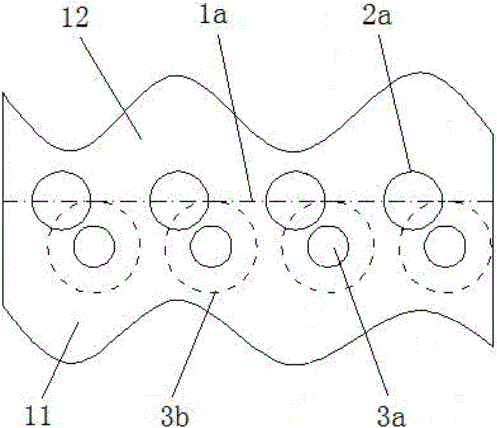
[0061] ② Drilling: drill a plated through hole 2a with a diameter of D on the boundary 1a between the removed area 11 and the reserved area 12 of the circuit board, and drill a guide away from the plated through hole 2a in the removed area 12 of the circuit board 1 Hole 3a, guide hole 3a diameter D1=0.7D, as figure 2 ;

[0062] ③Electroplating: Copper film 4 is plated on the surface of the circuit board;

[0063] ④ Circuit transfer: Apply exposure ink on the ci...

Embodiment 3

[0071] Such as Figure 6 As shown, the difference from Embodiment 2 is that the drill bit 71 for drilling plated through holes drills through the circuit board 1 , and then the drill bit 72 for drilling pilot holes drills through the circuit board 1 . Because the plated through hole 2a is a hole that actually needs to be reserved, and the guide hole 3a is a hole that will be eliminated, so the position accuracy of the plated through hole 2a is required to be higher, and it needs to be drilled out first. After the plated through-hole drill bit 71 drills through the circuit board 1 first, the circuit board 1 can be released from stress and returned to be flat, so that the circuit board 1 will not be broken due to excessive force at the same time when the pilot hole 3a is drilled.


PUM


Abstract

The invention belongs to the technical field of fabrication of a printed circuit board (PCB), and relates to a forming process of a burr-free PCB. The forming process sequentially comprises the following steps of substrate fabrication, plated through hole drilling, electroplating, circuit transfer-printing, hole drilling and breaking, circuit etching and milling. According to the forming process, the step of circuit etching is arranged after the step of hole drilling and breaking, burrs formed during hole drilling and breaking is corroded by a corrosion reagent, the burr problem also can be solved although the step of processing is not added, and the qualified rate of circuit board drilling is improved.

Description

technical field [0001] The invention relates to the technical field of printed circuit board manufacturing, in particular to a burr-free PCB molding process with high yield. Background technique [0002] The half hole is cut in half on the basis of the plated through hole. It is located on the edge of the printed circuit board. It not only retains the conduction function of the original plated through hole, but also uses the half hole wall for welding and fixing, realizing the board The simple and high-strength fixing to the board or parts is widely used. [0003] The traditional semi-hole plate manufacturing process is: image transfer→graphic plating→film removal→etching→solder mask→surface coating→half hole and shape are formed at the same time. This kind of half hole is formed by cutting the circular plated through hole in half directly after the circular plated through hole is formed. Due to the better ductility of the copper in the hole and the pulling caused by mechan...

Claims


Application Information

Patent Timeline
Patent Type & Authority Applications(China)
IPC IPC(8): H05K3/42
CPCH05K3/42H05K2203/0221H05K2203/14
Inventor 赖荣祥
Owner PLOTECH TECH KUNSHAN CO LTD
Why Eureka
Try Eureka