Unidirectional optical transmitting method and apparatus for photonic crystal based all-optical diode

An all-optical diode and photonic crystal technology, which is applied in the field of all-optical non-reciprocal optical transmission, can solve the problems of unfavorable photodiode high-speed response, unfavorable photonic chip integration, and low forward transmittance, achieving high flexibility and freedom , high contrast, large working bandwidth effect

Active Publication Date: 2016-06-29
SOUTH CHINA UNIV OF TECH
View PDF7 Cites 9 Cited by
  • Summary
  • Abstract
  • Description
  • Claims
  • Application Information

AI Technical Summary

Problems solved by technology

In 2012, Weiner, a member of the American Academy of Sciences, and Professor Qi Minghao from Purdue University proposed an asymmetric Si-based microring resonator-waveguide structure, which achieved a forward and reverse light transmission contrast of 27dB when the incident power was 2.1 mW. , but the forward transmittance i

Method used


Image

  • Unidirectional optical transmitting method and apparatus for photonic crystal based all-optical diode
  • Unidirectional optical transmitting method and apparatus for photonic crystal based all-optical diode
  • Unidirectional optical transmitting method and apparatus for photonic crystal based all-optical diode

Examples


Embodiment 1

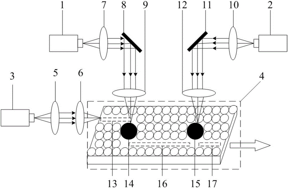
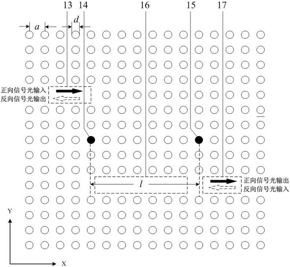
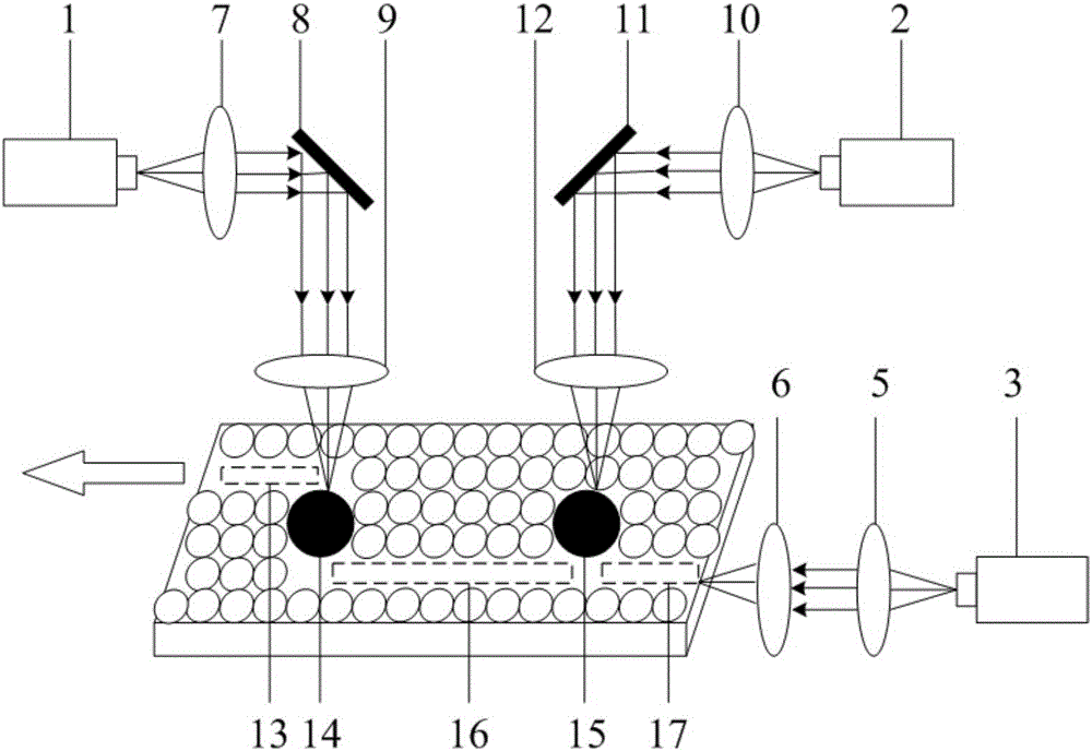
[0034] Such as figure 1As shown, the unidirectional optical transmission device based on the photonic crystal all-optical diode of the present embodiment includes a power tunable ultrashort pulse laser (PulsedLD) 1, a power tunable ultrashort pulse laser (PulsedLD) 2, a wavelength tunable continuous wave A laser (CWLD) 3, a photonic crystal-based all-optical diode 4, and a 50× microscope objective lens 5, 50 are sequentially arranged between the wavelength-tunable continuous wave laser 3 and the front-side photonic crystal waveguide 13 of the photonic crystal-based all-optical diode ×microscopic objective lens 6; between the power adjustable ultrashort pulse laser 1 and the direct coupling microcavity 14 based on the photonic crystal all-optical diode, a 50×microscopic objective lens 7, a mirror 8, and a 50×display are sequentially arranged along the direction of the optical path. Micro-objective lens 9; a 50×microscopic objective lens 10, a mirror 11, and a 50×microscopic len...

Embodiment 2

[0043] In this embodiment, the all-optical diode that realizes light transmission with high reverse transmittance and low forward transmittance is the same as that of Embodiment 1 except for the following features.

[0044] Adjust the power of the two power-tunable ultrashort pulse lasers to 20 W and 9 W, respectively.

[0045] The signal light emitted by the wavelength-tunable continuous wave laser is injected into the front side linear photonic crystal waveguide of the photonic crystal-based all-optical diode (ie, forward incidence) along the 2-dimensional linear photonic crystal plane (ie, the xy plane), and the nonlinear Kerr Under the effect, both the direct-coupled microcavity and the side-coupled microcavity will be in a high-energy state. However, since the resonant wavelength of the side-coupling microcavity is red-shifted and exactly equal to the wavelength of the incident signal light, the signal light will be reflected back by the side-coupling microcavity with a h...


PUM


Abstract

The invention discloses a unidirectional optical transmitting method for a photonic crystal based all-optical diode. A direct coupling micro cavity and a side coupling micro cavity of the photonic crystal are pumped by two ultra-short pulse laser with adjustable power respectively, wherein the direct coupling micro cavity is taken as a variable transmission unit while the side coupling micro cavity is taken as a variable reflection unit; multiple combinations of optical dual stable states, including a high-energy state and a low-energy state, of the two micro cavities can be realized by choosing proper pulse pumping power based on a nonlinear Kerr effect; and the incident continuous wave signal is subjected to the dual regulation and control by the two micro cavities, so that the forward high transmission or backward high transmission of the all-optical diode can be realized. The invention also discloses a unidirectional optical transmitting apparatus for the photonic crystal based all-optical diode. The pass-through directions of the signal light can be freely controlled by adjusting the pumping power of the ultra-short pulse laser; and extremely high forward transmission and backward transmission contrast ratio and relatively high operating bandwidth can be obtained.

Description

technical field [0001] The invention relates to all-optical non-reciprocal light transmission technology, in particular to a method and device for one-way light transmission of all-optical diodes based on a photonic crystal. Background technique [0002] All-optical diode is an important micro-nano optical device. Its non-reciprocal structure allows signal light to pass in one direction, while in the opposite direction, it passes little or almost nothing. In short, it realizes one-way light transmission. However, the development of high-performance all-photodiodes is a worldwide problem in the field of micro-nano integrated photonics. Just as the basic element of the electric diode is needed for the operation function of the traditional integrated circuit system, the operation and processing of the all-optical signal is also inseparable from the unit that can make the photon meet the non-reciprocal transmission, the so-called all-optical diode. At the same time, the rapid ...

Claims


Application Information

Patent Timeline
IPC IPC(8): H01S3/10H01S3/08H01S3/094G02B6/122G02F3/02
CPCH01S3/08H01S3/094076H01S3/10H01S3/1024G02F3/026G02B6/1225
Inventor 李潮王敏吴俊芳
Owner SOUTH CHINA UNIV OF TECH
Why Eureka
Try Eureka