Polycrystalline silicon ingot and production method thereof

A technology of polycrystalline silicon ingots and seed crystals, applied in the field of polycrystalline silicon ingots and its preparation, can solve the problems of high crystal defect density, reduced electrical performance, and unstable crystallization direction in the edge area of ​​​​silicon ingots, so as to reduce the defect density and impurities of silicon crystals content, reduce crystal defects, the effect of reasonable and easy method

Active Publication Date: 2016-07-13
JIANGXI SAI WEI LDK SOLAR HI TECH CO LTD
View PDF5 Cites 7 Cited by
  • Summary
  • Abstract
  • Description
  • Claims
  • Application Information

AI Technical Summary

Problems solved by technology

[0003] However, due to factors such as poor thermal conductivity of the crucible and unstable crystallization direction in the corner area of ​​the polycrystalline silicon ingot produced by the existing polycrystalline silicon casting method, the density of crystal defects in the edge area of ​​the silicon ingot is relatively high, resulting i...

Method used


Image

  • Polycrystalline silicon ingot and production method thereof
  • Polycrystalline silicon ingot and production method thereof
  • Polycrystalline silicon ingot and production method thereof

Examples


Embodiment 1

[0029] A method for preparing a polycrystalline silicon ingot, comprising the following steps:

[0030] (1) In the center of the bottom of the crucible, the average dislocation density is 1×10 3 / cm 2 common seed crystals to form a first seed layer with a thickness of 3 cm, and then lay an average dislocation density of 1×10 6 / cm 2 The seed crystal with high-density crystal defects forms a second seed crystal layer with a width of 3 cm and a thickness of 3 cm; the second seed crystal layer is formed around the first seed crystal layer, and the first seed crystal layer and the second seed crystal layer completely cover the bottom of the crucible;

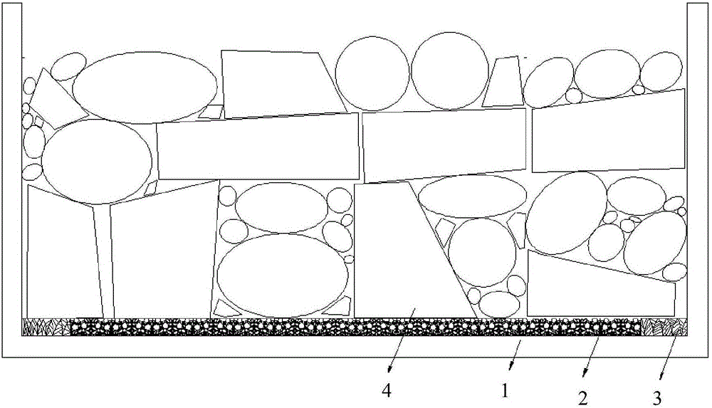
[0031] figure 2 It is a schematic diagram of laying the first seed layer and the second seed layer on the bottom of the crucible in the present invention, wherein 1 is the crucible, 2 is the first seed layer, 3 is the second seed layer, and 4 is silicon material.

[0032] (2) setting molten silicon material on the first seed c...

Embodiment 2

[0040] A method for preparing a polycrystalline silicon ingot, comprising the following steps:

[0041] (1) In the center of the bottom of the crucible, the average dislocation density is 1×10 3 / cm 2 Common seed crystals form a first seed layer with a thickness of 2cm, and then lay an average dislocation density of 1×10 6 / cm 2 A seed crystal with a high density of crystal defects forms a second seed crystal layer with a width of 2 cm and a thickness of 2 cm; the second seed crystal layer is formed around the first seed crystal layer, and the first seed crystal layer and the second seed crystal layer completely cover the bottom of the crucible;

[0042] (2) setting molten silicon material on the first seed crystal layer and the second seed crystal layer, controlling the temperature at the bottom of the crucible so that the first seed crystal layer and the second seed crystal layer are not completely melted;

[0043] (3) Control the thermal field in the crucible to form a ...

Embodiment 3

[0046] A method for preparing a polycrystalline silicon ingot, comprising the following steps:

[0047] (1) In the center of the bottom of the crucible, the average dislocation density is 1×10 3 / cm 2 Ordinary seed crystals form a first seed layer with a thickness of 3 cm, and lay an average dislocation density of 1×10 on the bottom of the crucible near the side wall 6 / cm 2 A seed crystal with a high density of crystal defects forms a second seed layer with a width of 3 cm and a thickness of 2 cm; and then lays an average dislocation density of 1×10 on the second seed layer. 3 / cm 2 The ordinary seed crystal formation width is 3cm, the third seed crystal layer is 1cm thick, the second seed crystal layer and the third seed crystal layer are formed around the first seed crystal layer, and the first seed crystal layer and the second seed crystal layer are completely Cover the bottom of the crucible;

[0048] (2) setting molten silicon material on the first seed crystal laye...


PUM

PropertyMeasurementUnit
Thicknessaaaaaaaaaa
Thicknessaaaaaaaaaa
Thicknessaaaaaaaaaa

Abstract

The invention provides a production method of a polycrystalline silicon ingot, comprising: laying common seed crystal at the bottom center of a crucible to form a first seed crystal layer, and laying seed crystal with high-density crystal defect at the bottom of the crucible approximate to the sidewall of the crucible to form a second seed crystal layer; placing molten silicon material on the first seed crystal layer and the second seed crystal layer, and controlling the temperature of the bottom of the crucible so that the first and second seed crystal layers are not completely melted; controlling a heat field in the crucible to from a degree of supercooling, controlling the temperature in the crucible to rise gradually in a direction upwardly perpendicular to the bottom of the crucible to form a temperature gradient so that the melted silicon material crystallizes and solidifies, and annealing and cooling to obtain polycrystalline silicon ingot after complete crystallization.The silicon crystal density and impurity content of an edge area of the silicon ingot can be effectively reduced, and overall quality of the silicon ingot can be effectively improved.The invention also provides the polycrystalline ingot prepared using the method.

Description

technical field [0001] The invention relates to the field of polycrystalline silicon ingots, in particular to a polycrystalline silicon ingot and a preparation method thereof. Background technique [0002] At present, in the casting polycrystalline market, high-efficiency polycrystalline silicon wafers occupy a major position. High-efficiency polycrystalline casting mainly includes two methods: full-melt method and semi-melt method. After the material is melted, it nucleates and crystallizes on the seed crystal to form a polycrystalline silicon ingot. [0003] However, due to factors such as poor thermal conductivity of the crucible and unstable crystallization direction in the corner area of ​​the polycrystalline silicon ingot produced by the existing polycrystalline silicon casting method, the density of crystal defects in the edge area of ​​the silicon ingot is relatively high, resulting in the silicon ingot in this area. The conversion efficiency of the solar cell is lo...

Claims


Application Information

Patent Timeline
IPC IPC(8): C30B28/06C30B29/06
CPCC30B28/06C30B29/06
Inventor 雷琦胡动力何亮张学日
Owner JIANGXI SAI WEI LDK SOLAR HI TECH CO LTD
Why Eureka
Try Eureka