Laser array beam combining device

A laser array and laser beam technology, applied in the field of lasers, can solve the problems of long adjustment difficulty, inconvenient expansion of semiconductor laser power, and high stability requirements

Inactive Publication Date: 2016-07-27
II VI SUWTECH INC
View PDF11 Cites 25 Cited by
  • Summary
  • Abstract
  • Description
  • Claims
  • Application Information

AI Technical Summary

Problems solved by technology

[0009] However, based on U.S. Patent No. 6,192,062 and similar technologies, the spectral combination of external cavity semiconductor laser arrays has a narrow spectrum of a single laser; and due to the long overall optical path, it is difficult to adjust...

Method used


Image

  • Laser array beam combining device
  • Laser array beam combining device
  • Laser array beam combining device

Examples


no. 1 example

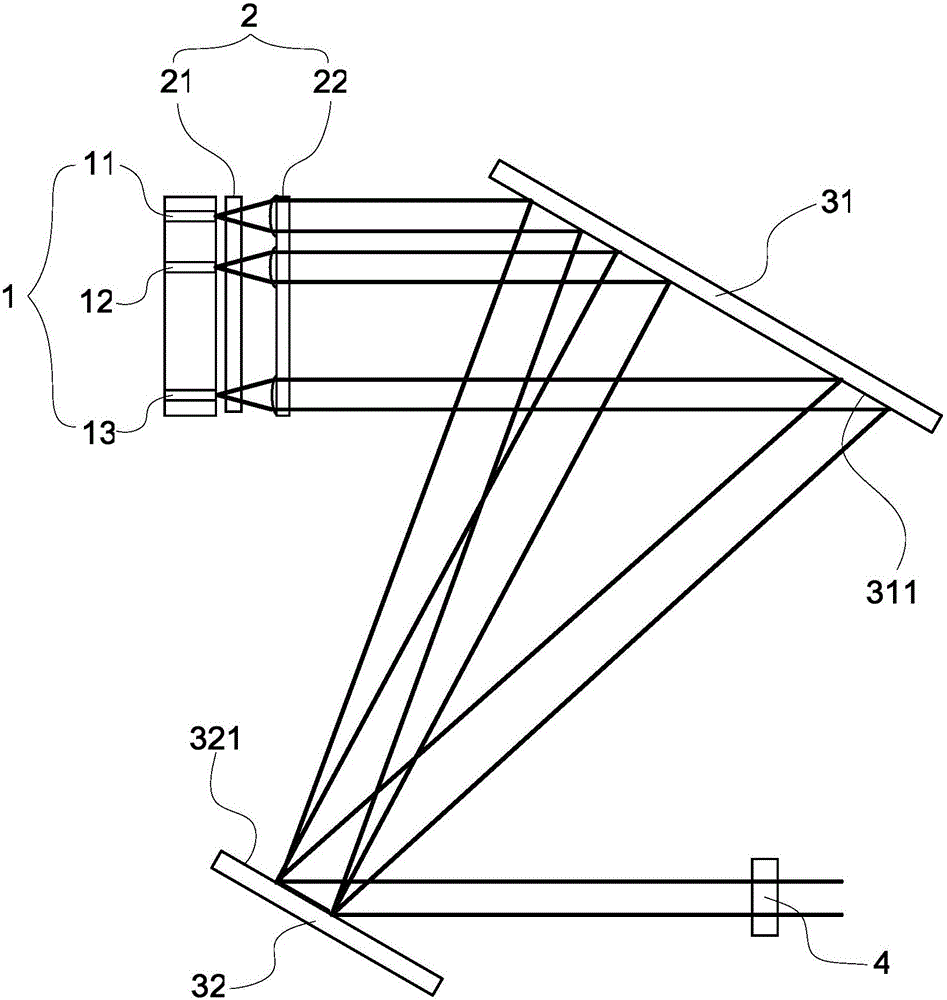
[0034] See figure 1 , Which shows a schematic structural diagram of the laser array beam combining device of the first embodiment of the present invention. in figure 1 In the preferred embodiment shown, the laser array beam combining device includes: a laser gain medium array 1, a shaping optical system 2, a dispersive optical component, and a partially reflective optical element 4.

[0035] The laser gain medium array 1 includes at least two laser gain elements, each of which can generate a laser beam with a certain spectral width. in figure 1 In the illustrated embodiment, the laser gain medium array 1 is preferably a semiconductor laser array. The laser gain medium array 1 includes multiple laser gain elements. It should be noted that, figure 1 Only the first laser gain element 11, the second laser gain element 12, and the third laser gain element 13 are schematically shown in, where the third laser gain element 13 is n laser gain elements spaced from the second laser gain ele...

no. 2 example

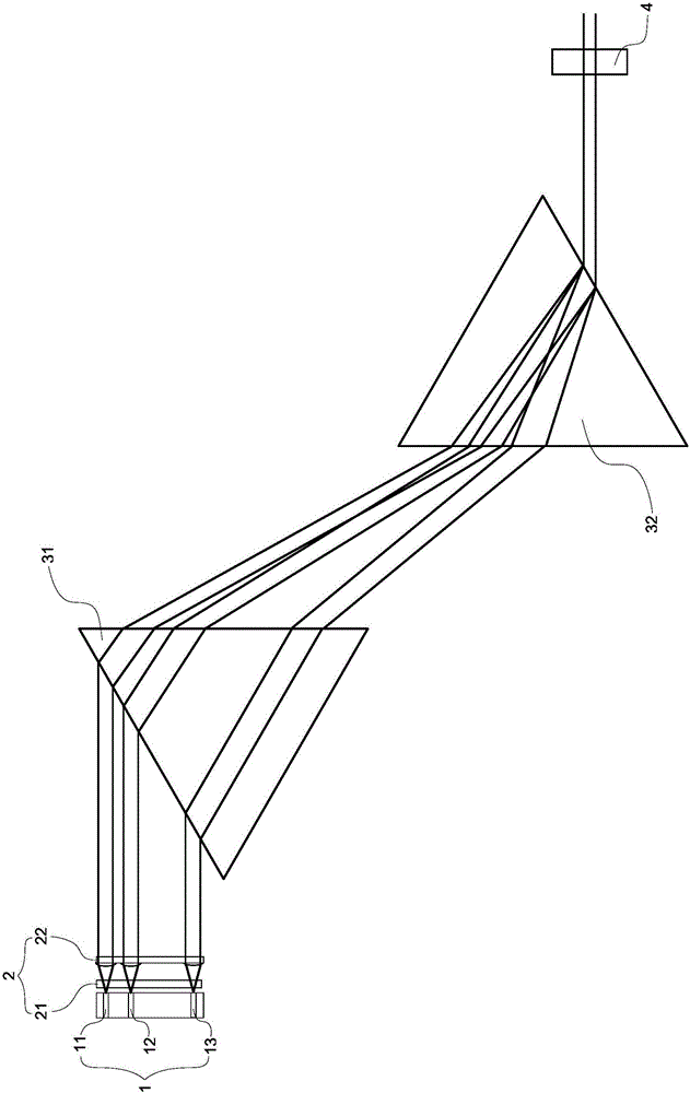
[0041] See figure 2 , Which shows a schematic structural diagram of the laser array beam combining device of the second embodiment of the present invention. With the above figure 1 The difference in the first embodiment shown is that in this embodiment, the first dispersive optical element and the second dispersive optical element are a pair of diffraction gratings. The first dispersive optical element and the second dispersive optical element use a pair of diffraction gratings instead of the prism pair in the above-mentioned first embodiment. Specifically, such as figure 2 As shown, the first dispersive optical element 31' and the second dispersive optical element 32' are a pair of diffraction gratings. The diffraction grating may be a transmissive grating or a reflective grating. Preferably, the grating surfaces of the pair of diffraction gratings are parallel to each other and have the same grating period. This embodiment can achieve similar effects to the above-mentione...

no. 3 example

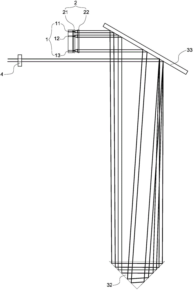
[0043] See image 3 , Which shows a schematic structural diagram of a laser array beam combining device according to a third embodiment of the present invention. With the above figure 1 with figure 2 The difference between the first embodiment and the second embodiment shown is that in this embodiment, the dispersive optical component includes a third dispersive optical element and a reflective prism. The dispersive optical component uses the third dispersive optical element and the reflective prism to replace the above-mentioned first dispersive optical element and the second dispersive optical element. Specifically, such as image 3 As shown, the dispersive optical component includes a third dispersive optical element 33 and a reflective prism 34. The third dispersive optical element 33 diffracts or refracts the collimated laser beam array incident by the shaping optical system 2. in image 3 In the illustrated embodiment, the third dispersive optical element 33 is a dif...


PUM


Abstract

The invention discloses a laser array beam combining device, which comprises a laser gain medium array, a shaping optical system, a dispersing optical component and a partial reflecting optical component, wherein the laser gain medium array comprises at least two laser gain elements; each laser gain element can generate a laser beam with a certain spectrum width; the shaping optical system is used for collimating each laser beam generated by the laser gain medium array to obtain a group of parallel collimated laser beam arrays; the dispersing optical component is used for carrying out at least two diffraction or refraction on the incident collimated laser beam arrays and then combining the beams for outputting; and the partial reflecting optical component is used for receiving the combined laser beams and ejecting the laser beams.

Description

Technical field [0001] The invention relates to the field of lasers, in particular to a beam combining device with a spectrum overlapping external cavity laser array. Background technique [0002] Semiconductor lasers have the characteristics of high efficiency, small size, wide wavelength range, low cost, and high reliability. Compared to other lasers, they are very attractive. However, the output beam quality of the semiconductor laser is poor, and the power level of a single laser is limited, which hinders the expansion of its application range. [0003] In recent years, with the development of semiconductor laser technology, and driven by the demand for direct semiconductor laser industrial processing and high-power fiber laser pumping, semiconductor lasers with high power and high beam quality have developed rapidly. At the same time, laser beam combining technology has doubled the laser power in the past few years. At present, the power levels of fiber lasers and direct sem...

Claims


Application Information

Patent Timeline
IPC IPC(8): H01S5/40H01S5/10G02B27/10G02B27/30
CPCG02B27/10H01S5/10H01S5/40H01S5/4025G02B27/30
Inventor 张哨峰李大汕杨金涛沈渊孙晓斌
Owner II VI SUWTECH INC
Why Eureka
Try Eureka