

Large-current silicon on insulator lateral insulated gate bipolar transistor device
A bipolar transistor, silicon-on-insulator technology, applied in semiconductor devices, electrical components, circuits, etc., can solve problems such as destructive failure of device structure, thermal breakdown of devices, and reduced latch-up suppression capability, and reduce electron aggregation. level, the effect of improving the on-current density, and improving the latch-up suppression capability
- Summary
- Abstract
- Description
- Claims
- Application Information
AI Technical Summary
Problems solved by technology
Method used
Image

Examples
Embodiment Construction
[0028] Combine below figure 2 , image 3 , Figure 4 , the present invention is described in detail:
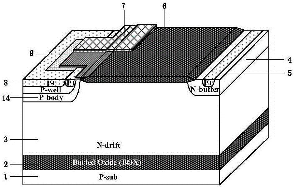
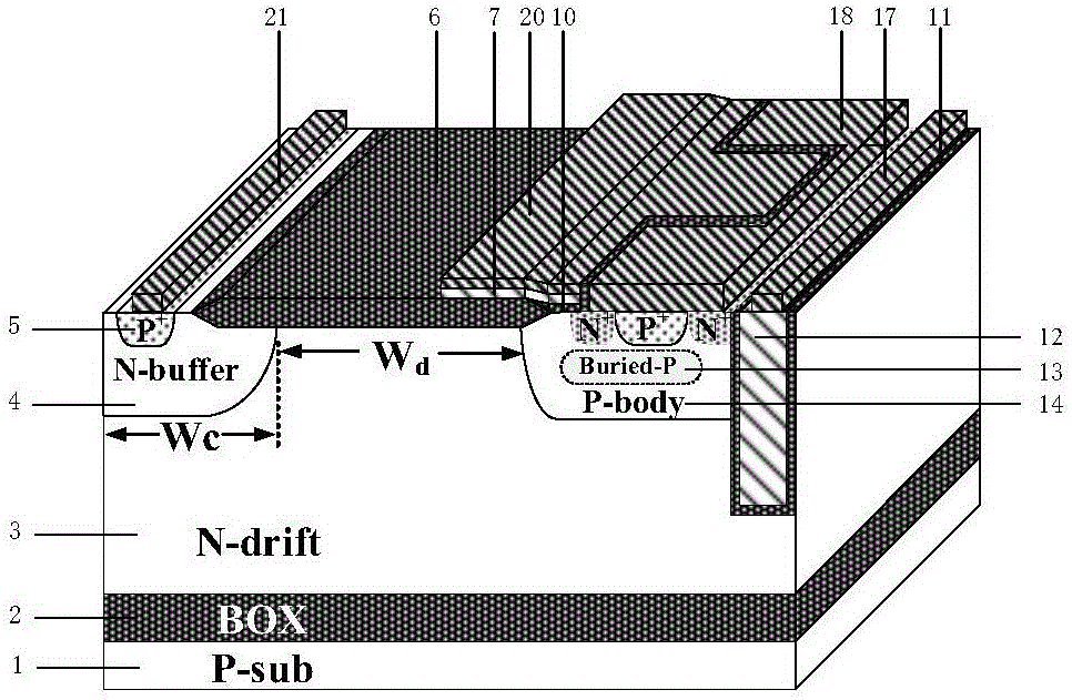
[0029] A large current silicon-on-insulator lateral insulated gate bipolar transistor device, comprising: a P-type substrate 1, a buried oxygen 2 is arranged on the P-type substrate 1, and an N-type drift region 3 is arranged on the buried oxygen 2, An N-type buffer zone 4 and a P-type body region 14 are respectively arranged on both sides of the N-type drift region 3, and a heavily doped P-type collector region 5 is arranged in the N-type buffer region 4, and a heavily doped P-type collector region 5 is arranged. A collector metal 21 is connected to the electrode region 5, a heavily doped P-type emitter region 8 is provided in the P-type body region 14, and a heavily doped P-type emitter region 8 is provided around the heavily doped P-type emitter region 8. The N-type emitter region 9 is connected with the emitter metal 18 on the above-mentioned heavily doped P-type emit...
PUM
 Abstract
Description
Claims
Application Information