Separately-shielded and symmetrically-stranded cable resistant to high temperature and with low noise and fabrication method thereof
A manufacturing method and high-temperature-resistant technology, applied to power cables with shielding/conductive layers, insulated cables, flat/ribbon cables, etc., can solve the problems of piezoelectric effect, poor cable temperature adaptability, and easy damage And other issues
- Summary
- Abstract
- Description
- Claims
- Application Information
AI Technical Summary
Problems solved by technology
Method used
Image
Examples
Embodiment 1
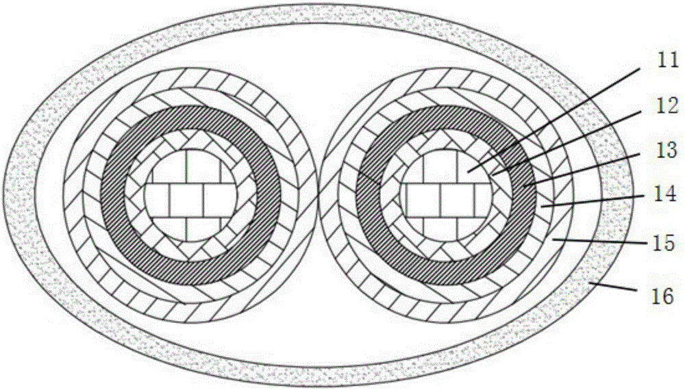
[0042] figure 1 A structural schematic diagram of a sub-shielded symmetrical twisted high temperature resistant low noise cable provided for the embodiment of the present invention; figure 1 As shown, a sub-shielded symmetrical twisted high-temperature-resistant low-noise cable provided in this embodiment includes: at least one pair of conductors 11, and the conductors 11 are covered in a fluoroplastic sheath 16;
[0043] The conductor 11 is covered with a first semiconductor layer 12 , a first fluoroplastic insulating layer 13 , a second semiconductor layer 14 and a sub-shielding layer 15 from inside to outside.
[0044] The gap between the sub-shielding layer 15 and the fluoroplastic sheath 16 is filled with a gel-like substance.
[0045] The conductor 11 is at least one pair. This embodiment adopts a pair of conductors 11, and can also be set as multiple pairs of conductors 11 according to actual use requirements. The double-conductor arrangement can reduce the interference ...
Embodiment approach
[0077] As the second embodiment of the present invention, it is another implementation of the first embodiment of the present invention, that is, the gap between the shielding layer and the fluoroplastic sheath is filled with hot melt adhesive, and the fluoroplastic sheath The cross-section adopts circular ring design.
[0078] A symmetrically stranded high-temperature-resistant low-noise cable of the present invention includes: at least one pair of conductors 11, the conductors 11 are covered in a fluoroplastic sheath 16;
[0079] The conductor 11 is covered with a first semiconductor layer 12, a first fluoroplastic insulating layer 13, a second semiconductor layer 14 and a sub-shielding layer 15 from inside to outside;
[0080] The gap between the sub-shielding layer 15 and the fluoroplastic sheath 16 is filled with hot melt adhesive.
[0081] The cross-section of the fluoroplastic sheath 16 is circular.
[0082] The hot-melt adhesive is a kind of plastic adhesive. Its physi...
PUM
 Abstract
Description
Claims
Application Information

