Preparation method for silicon photocatalyst with 3D multilevel structure

A catalyst and silicon photonics technology, applied in chemical instruments and methods, physical/chemical process catalysts, chemical/physical processes, etc., can solve the problem of limiting the application of silicon materials, the inability to effectively reduce the reflection of silicon materials, and the energy efficiency is not very significant, etc. problems, to achieve the effect of short preparation period, low cost and easy control

Inactive Publication Date: 2016-08-17
DALIAN UNIV OF TECH
View PDF3 Cites 2 Cited by
  • Summary
  • Abstract
  • Description
  • Claims
  • Application Information

AI Technical Summary

Problems solved by technology

However, the morphology and structure of silicon materials that are more commonly studied now are generally nanowires, quantum dots, nanorods, porous silicon, etc. These morphology structures are not very sign...

Method used


Image

  • Preparation method for silicon photocatalyst with 3D multilevel structure
  • Preparation method for silicon photocatalyst with 3D multilevel structure
  • Preparation method for silicon photocatalyst with 3D multilevel structure

Examples


Embodiment 1

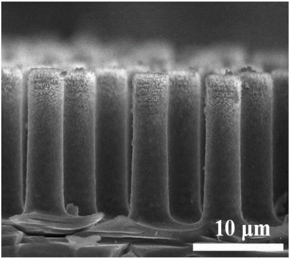
[0026] A method for preparing a silicon photocatalyst with a 3D multilevel structure, the steps are as follows:

[0027] (1) At room temperature, the silicon column array was ultrasonically cleaned in acetone, absolute ethanol and high-purity water, and then the ultrasonically cleaned silicon column array was placed in a volume ratio of 3:1 H 2 SO 4 and H 2 o 2 Soak in the mixed solution for 15 minutes, rinse the obtained silicon column array with high-purity water repeatedly, then place it in 5% HF aqueous solution at room temperature, and soak for 1 minute to remove impurities and natural oxide layer on the silicon surface;

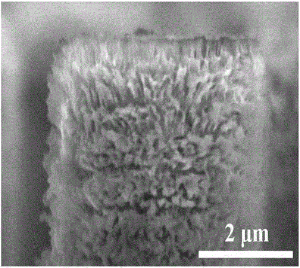
[0028] (2) Place the silicon column array obtained in step (1) into 30mL of 4.2M HF and 0.005M AgNO 3 In the mixed solution, the temperature of the water bath is 30°C, and the etching is performed for 25 minutes to obtain multi-level silicon;

[0029] (3) The multi-level silicon obtained in step (2) was washed repeatedly with high-purity water, and ...

Embodiment 2

[0036] (1) At room temperature, the silicon column array was ultrasonically cleaned in acetone, absolute ethanol and high-purity water, and then the ultrasonically cleaned silicon column array was placed in a volume ratio of 3:1 H 2 SO 4 and H 2 o 2 Soak in the mixed solution for 15 minutes, rinse the obtained silicon column array with high-purity water repeatedly, and then place it in an aqueous HF solution with a volume fraction of 5% at room temperature, and soak for 1 minute to remove impurities and natural oxide layers on the silicon surface;

[0037](2) Place the silicon column array obtained in step (1) into 30mL of 4.2M HF and 0.005M AgNO 3 In the mixed solution, the temperature of the water bath is 30°C, and the etching is performed for 10 minutes to obtain multi-level silicon;

[0038] (3) The multi-level silicon obtained in step (2) was washed repeatedly with high-purity water, and then placed in 20 mL of HNO with a molar concentration of 7.66M 3 In the aqueous ...

Embodiment 3

[0041] (1) At room temperature, the silicon column array was ultrasonically cleaned in acetone, absolute ethanol and high-purity water, and then the ultrasonically cleaned silicon column array was placed in a volume ratio of 3:1 H 2 SO 4 and H 2 o 2 Soak in the mixed solution for 15 minutes, rinse the obtained silicon column array with high-purity water repeatedly, and then place it in an aqueous HF solution with a volume fraction of 5% at room temperature, and soak for 1 minute to remove impurities and natural oxide layers on the silicon surface;

[0042] (2) Place the silicon column array obtained in step (1) into 30mL of 4.2M HF and 0.005M AgNO 3 In the mixed solution, the temperature of the water bath is 30°C, and the etching is carried out for 20 minutes to obtain multi-level silicon;

[0043] (3) The multi-level silicon obtained in step (2) was washed repeatedly with high-purity water, and then placed in 20 mL of HNO with a molar concentration of 7.66M 3 In the aqueo...


PUM


Abstract

The invention belongs to the technical field of semiconductor photocatalysis and relates to a preparation method for a silicon photocatalyst with a 3D multilevel structure. A silicon pillar array is subjected to a cleaning process and then is etched under the water bath temperature at 30 DEG C. The multi-level silicon is acquired by regulating the etching time. The light absorption strength of the prepared multi-level silicon is high; the light current is -30mAcm<2> and is 7.5 times of the light current of the silicon pillar array; 4-chlorophenol is dechlorinated under the photoelectric combined action; the dechlorinating efficiency can reach 90% or more after reacting for 60min; high-efficient photoelectric catalytic capacity is represented; the preparation method has the advantages of mild reaction condition, simple and convenient preparation technique, low cost, short preparation period, easy control, and the like; the prepared multi-level silicon photocatalyst can effectively enhance the light absorption of the material, reduce the light reflection, increase the light absorbing efficiency, boost the separation of photoproduced electron and hole and increase the photocatalytic activity; the effect in photoelectrocatalytic dechlorinating is obvious.

Description

technical field [0001] The invention belongs to the technical field of semiconductor photocatalysis, and relates to a method for preparing a silicon photocatalyst with a 3D multilevel structure. Background technique [0002] Photocatalytic technology can use strong oxidizing holes or hydroxyl radicals to completely decompose most pollutants. It has the advantages of environmental friendliness, complete pollutant degradation and mild reaction conditions, and is expected to use clean solar energy, so it is considered to be a pollutant. One of the most promising new technologies in the field of control. However, the low utilization rate of light energy limits the practical application of photocatalytic technology. Therefore, how to improve energy efficiency is a key scientific problem faced by photocatalytic technology. Aiming at the scientific problem of how to improve the light absorption efficiency, the solution mainly includes constructing a special surface structure to re...

Claims


Application Information

Patent Timeline
IPC IPC(8): B01J23/50
CPCB01J23/50B01J35/004
Inventor 全燮范凤杰于洪涛陈硕
Owner DALIAN UNIV OF TECH
Why Eureka
Try Eureka