Molybdenum and silicon substrate welding method in field emission device

A field emission device, silicon substrate technology, used in welding equipment, electric solid state devices, semiconductor devices, etc., can solve the problems of silicon wafer tearing, low welding strength, large deformation, etc., so that the connection will not break, improve Welding strength and the effect of blocking solder

Active Publication Date: 2016-08-17
UNIV OF ELECTRONICS SCI & TECH OF CHINA
View PDF3 Cites 1 Cited by
  • Summary
  • Abstract
  • Description
  • Claims
  • Application Information

AI Technical Summary

Problems solved by technology

[0004] Aiming at the deficiencies of the prior art, the present invention provides a method for welding molybdenum and silicon substrates in a field emission device, which solves the shortcomings of the existing solder that easily tears the silicon wafer, low welding strength, and large deformation. Greatly improve welding strength and product performance

Method used


Image

  • Molybdenum and silicon substrate welding method in field emission device
  • Molybdenum and silicon substrate welding method in field emission device
  • Molybdenum and silicon substrate welding method in field emission device

Examples


Embodiment 1

[0027] (1) Perform high-temperature vacuum annealing on the molybdenum sheet, the annealing temperature is 1000°C, and the annealing time is 20 minutes;

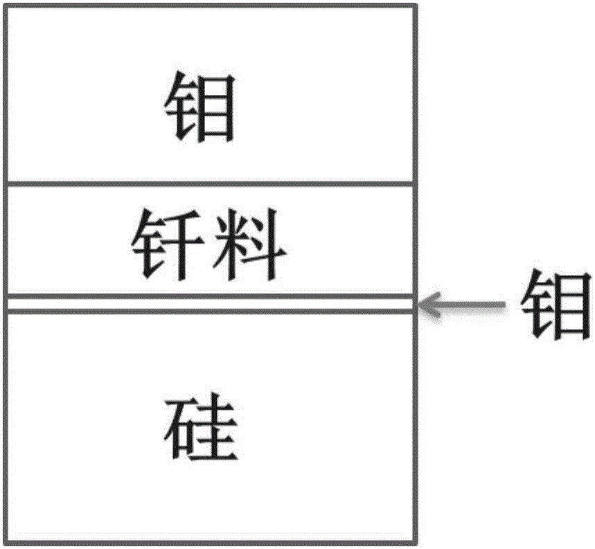
[0028] (2) Evaporate molybdenum thin film on silicon substrate by conventional thin film deposition method, and the system vacuum degree is 5×10 -4 Pa, molybdenum film thickness is 600nm;

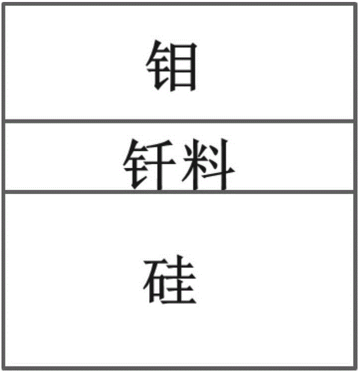
[0029] (3) The silicon substrate, copper-silver alloy sheet (silver-copper 28 welding sheet), and molybdenum sheet after molybdenum plating are stacked in sequence in a sintering furnace for high-vacuum sintering with a vacuum degree of 6×10 -4 Pa, the sintering temperature is 700°C, the holding time is 2min, the thickness of the silver-copper alloy is 0.03mm, and the thickness of the molybdenum sheet is 0.01mm.

Embodiment 2

[0031] (1) Carry out high-temperature vacuum annealing on the molybdenum sheet, the annealing temperature is 1200°C, and the annealing time is 60min;

[0032] (2) A molybdenum film was evaporated on a silicon substrate by a conventional film deposition method, and the vacuum degree of the system was 4×10 -4 Pa, molybdenum film thickness is 600nm;

[0033] (3) The silicon substrate, copper-silver alloy sheet (silver-copper 28 welding sheet), and molybdenum sheet after molybdenum plating are stacked in sequence in a sintering furnace for high-vacuum sintering with a vacuum degree of 4×10 -4 Pa, the sintering temperature is 800°C, the holding time is 2min, the thickness of the silver-copper alloy is 0.09mm, and the thickness of the molybdenum sheet is 0.09mm.

Embodiment 3

[0035] (1) Carry out high-temperature vacuum annealing on the molybdenum sheet, the annealing temperature is 1100°C, and the annealing time is 30min;

[0036] (2) Evaporate molybdenum thin film on silicon substrate by conventional thin film deposition method, the system vacuum degree is 2×10 -4 Pa, molybdenum film thickness is 600nm;

[0037] (3) The silicon substrate, copper-silver alloy sheet (silver-copper 28 welding sheet), and molybdenum sheet after molybdenum plating are stacked in sequence in a sintering furnace for high-vacuum sintering with a vacuum degree of 5×10 -4 Pa, the sintering temperature is 800°C, the holding time is 2min, the thickness of the silver-copper alloy is 0.05mm, and the thickness of the molybdenum sheet is 0.04mm.


PUM

PropertyMeasurementUnit
thicknessaaaaaaaaaa

Abstract

The invention provides a molybdenum and silicon substrate welding method in a field emission device. The method comprises the steps of evaporating a molybdenum thin film on a silicon substrate, and then welding the silicon substrate on which the molybdenum thin film is evaporated and a molybdenum plate, i.e., plating a molybdenum protecting layer on the silicon substrate to play a brazing filler metal barrier role. Silicon and the molybdenum plate are closely connected and cannot be broken, so the welding strength is greatly improved.

Description

technical field [0001] The invention belongs to the field of vacuum microelectronics, in particular to a method for welding molybdenum and silicon substrates in field emission devices. Background technique [0002] Vacuum microelectronic devices not only have the advantages of vacuum electronic devices such as radiation resistance, high temperature resistance, fast speed, high power, and low noise, but also have the advantages of small size, low power consumption, suitable for mass production, integration, and low cost of semiconductor devices. , is an ideal electronic device. The core component of vacuum microelectronic devices is the field emission array cathode, but the cathode cannot be directly used in practice, because the cathode usually uses silicon as the substrate, and the silicon material itself is very brittle and is easily damaged after being expanded by external friction. Molybdenum has the advantages of low thermal expansion coefficient, high thermal conducti...

Claims


Application Information

Patent Timeline
Patent Type & Authority Applications(China)
IPC IPC(8): H01L21/60B23K1/19B23K1/20
CPCB23K1/19B23K1/20H01L24/03H01L2224/03
Inventor 王小菊王旭聪马祥云曹贵川祁康成林祖伦
Owner UNIV OF ELECTRONICS SCI & TECH OF CHINA
Why Eureka
Try Eureka