A kind of bidirectional igbt device and manufacturing method thereof

A device and horizontal technology, applied in the field of power semiconductor devices, can solve the problems affecting the compromise characteristics of device switching loss, increasing device gate capacitance, and deteriorating short-circuit safe working area, etc.

Inactive Publication Date: 2018-11-09
UNIV OF ELECTRONICS SCI & TECH OF CHINA
View PDF4 Cites 0 Cited by
  • Summary
  • Abstract
  • Description
  • Claims
  • Application Information

AI Technical Summary

Problems solved by technology

However, for this bidirectional IGBT structure, when the forward or reverse IGBT works, the breakdown voltage of the device is significantly higher due to the higher doping concentration of the carrier storage layer and the existence of a certain thickness of the N-type layer 8 or 28. Reduce, in order to effectively shield the adverse effects of the N-type layer as the carrier storage layer and obtain a certain device withstand voltage, it is necessary to adopt: 1) deep trench gate depth, so that the depth of the trench gate is greater than the N-type layer 8 or 28 junction depth, but the deep trench gate depth not only increases the gate-emitter capacitance but also increases the gate-collector capacitance when working in either direction, thus reducing the switching speed of the device and increasing The switching loss of the device affects the compromise characteristics of the conduction voltage drop and switching loss of the device; 2) The small cell width makes the distance between the trench gates as small as possible, however, when working in any direction, the high The dense trench MOS structure not only increases the gate capacitance of the device, reduces the switching speed of the device, increases the switching loss of the device, and affects the compromise characteristics of the conduction voltage drop and switching loss of the device, but also, high The dense trench MOS structure increases the saturation current density of the device, making the short-circuit safe working area of ​​the device worse
Additionally, for figure 1 and 2 In the bidirectional IGBT structure shown, the gate oxide layer is formed in the trench by one-time thermal oxidation. In order to ensure a certain threshold voltage, the thickness of the entire gate oxide layer is small. Since the MOS capacitance is inversely proportional to the thickness of the oxide layer, traditional The small gate oxide thickness in the bidirectional IGBT structure greatly increases the gate capacitance of the device
In addition, the small gate oxide thickness concentrates the electric field at the bottom of the trench, making the device less reliable

Method used


Image

  • A kind of bidirectional igbt device and manufacturing method thereof
  • A kind of bidirectional igbt device and manufacturing method thereof
  • A kind of bidirectional igbt device and manufacturing method thereof

Examples


Embodiment 1

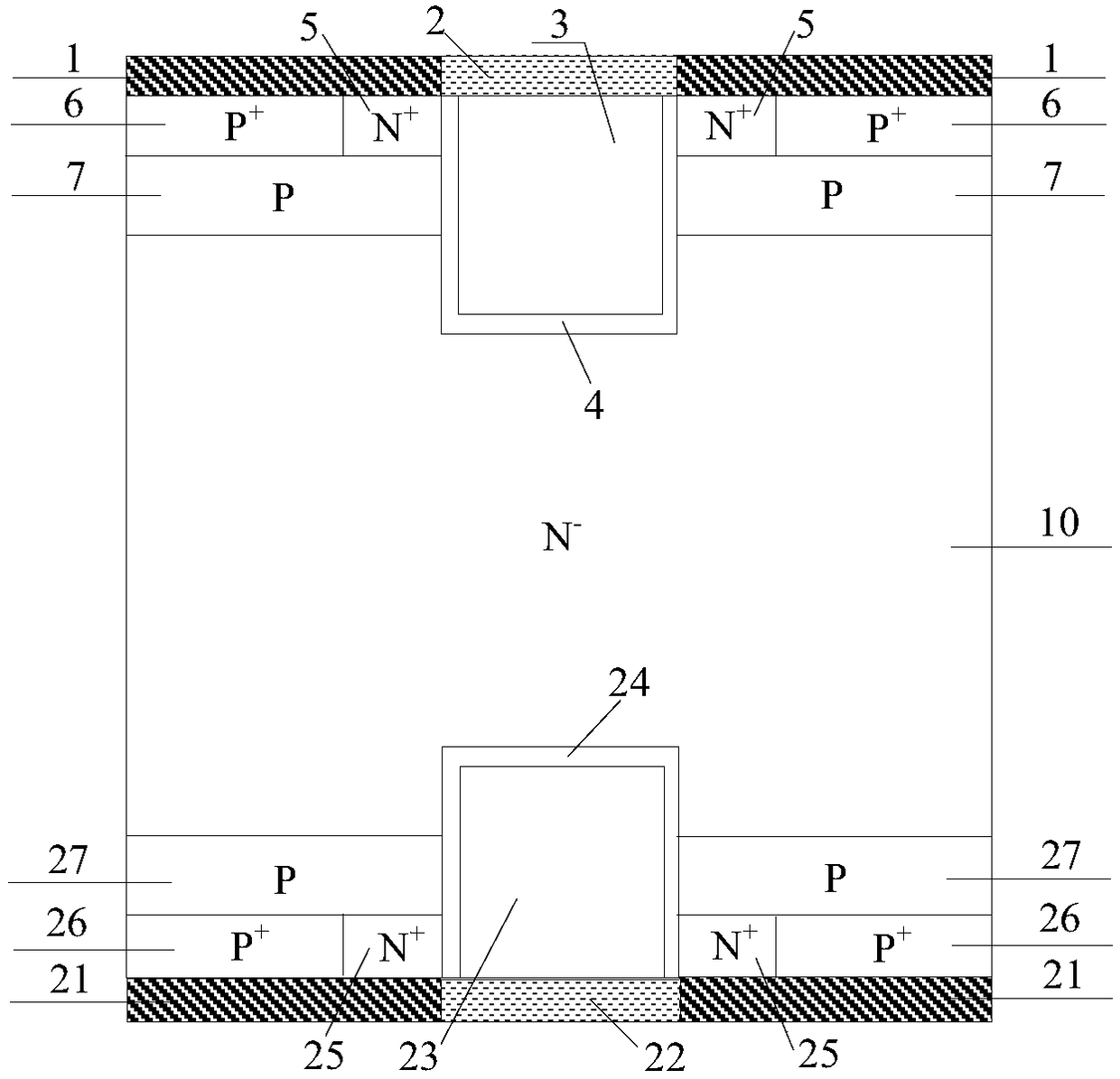
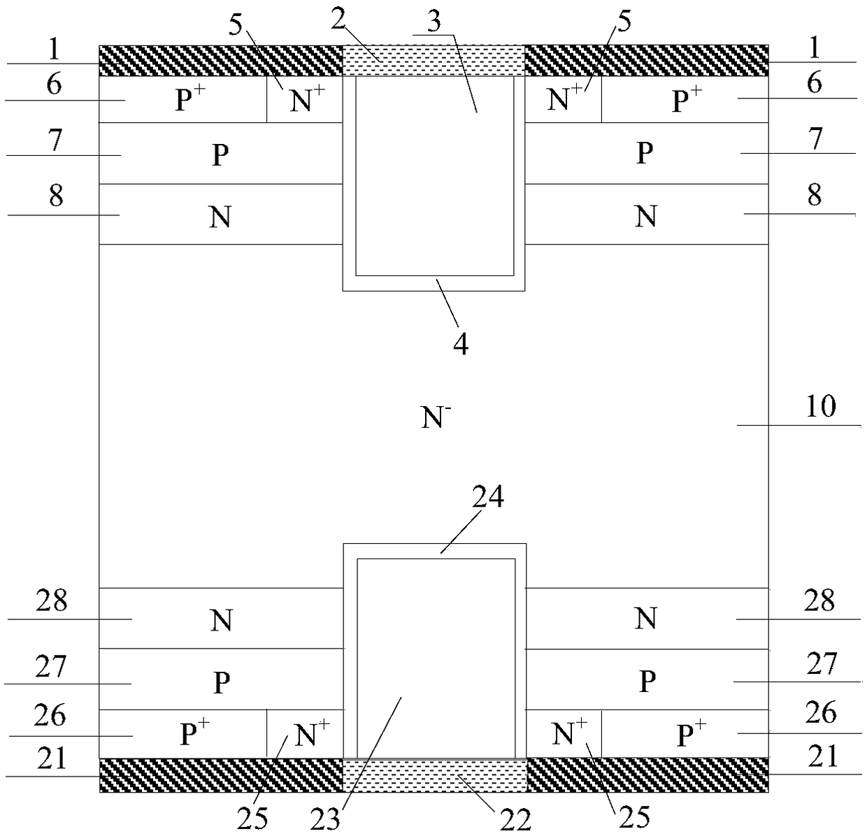
[0050] A bidirectional IGBT device with a cell structure such as image 3As shown, it includes two N-channel MOS structures symmetrically arranged on the front and back sides of the N-type drift region 10; the front MOS structure includes a front metal electrode 1, a front dielectric layer 2, a front N+ emitter region 5, and a front P+ emitter region 6. The front P-type base region 71, the front N-type layer 8 and the front trench gate structure; the back MOS structure includes the back metal electrode 21, the back first dielectric layer 22, the back N+ emitter region 25, and the back P+ emitter region 26 , the back P-type base region 271, the back N-type layer 28 and the back trench gate structure; it is characterized in that the front trench gate structure penetrates the front N-type layer 8 along the vertical direction of the device; the front P-type base region 71 On the upper surface of the front N-type layer 8 located on one side of the front trench gate structure, the f...

Embodiment 2

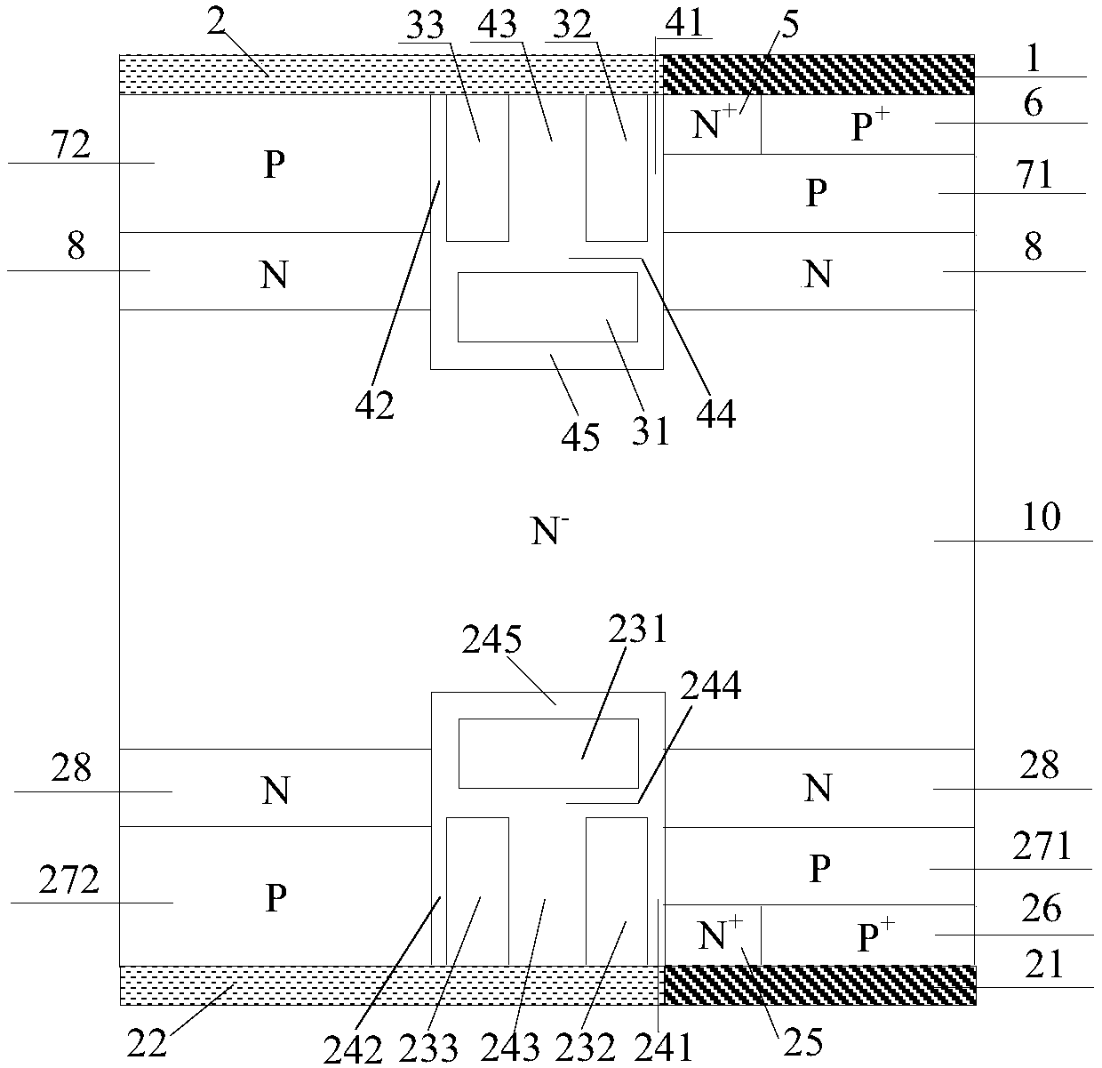
[0055] A bidirectional IGBT device in this example, its cell structure is as follows Figure 4 As shown, on the basis of Embodiment 1, the width of the front bottom split electrode 31 is greater than the front second dielectric layer 42, the front side split electrode 33, the front third dielectric layer 43, the front grid electrode 32 and the front grid dielectric layer 41. The sum of the widths makes the front compound trench gate structure an inverted "T" shape, that is, the width of the lower structure of the front compound trench structure is greater than the width of the upper structure and extends into the N-type layer 8; the back MOS The structure is connected and arranged mirror-symmetrically up and down along the center line of the N-type drift region 10 with the front MOS structure. The width of the underlying structure of the composite trench structure extending into the N-type layer 8 / 28 is about 1 / 4-3 / 4 of the width of the p-type base region 71 / 271 and the floati...

Embodiment 3

[0057] A bidirectional IGBT device in this example, its cell structure is as follows Figure 5 As shown, on the basis of Example 2, there is also a layer in the part of the region between the lower layer structure of the front / back composite trench structure and the p-type base region 71 / 271 and the floating p-type base region 72 / 272 N+ layer 9 / 29, the concentration of the N+ layer 9 / 29 is greater than the concentration of the N-type layer 8 / 28 and its sidewall is connected to the composite trench structure; one side of the N+ layer 9 / 29 is connected to the front N-type layer 8 / 28 connection, the other side and bottom of the N+ layer 9 / 29 are connected to the trench gate structure, the upper surface of the N+ layer 9 / 29 on one side of the trench gate structure is connected to the lower part of the floating P-type base region 72 / 272 Surface connection, the upper surface of the N+ layer 9 / 29 on the other side of the trench gate structure is connected to the lower surface of the ...


PUM


Abstract

A bidirectional IGBT device and a manufacturing method thereof belong to the technical field of power semiconductor devices. The present invention introduces a double-split electrode with the same potential as the metal electrode and a dielectric layer between the double-split electrode and the gate electrode at the bottom and side of the gate electrode in the trench on the front and back of the device, without affecting the threshold voltage and turn-on of the IGBT device. Under this condition, the symmetrical forward and reverse characteristics are realized, the forward and reverse switching speed of the bidirectional IGBT device is improved, and the switching loss of the device is reduced; the carrier concentration distribution of the entire N-type drift region is improved, and the forward conduction is improved. A compromise between voltage drop and switching loss; reduces the saturation current density of the device, improves the short-circuit safe working area of ​​the device, improves the concentration of the electric field at the bottom of the trench, increases the breakdown voltage of the device, and further improves the reliability of the device The bidirectional IGBT manufacturing method proposed in the present invention does not need to add additional process steps, and is compatible with the traditional bidirectional IGBT manufacturing method.

Description

technical field [0001] The invention belongs to the technical field of power semiconductor devices, and relates to an insulated gate bipolar transistor (IGBT), in particular to a bidirectional trench gate insulated gate bipolar transistor (Bi-directional trench IGBT). Background technique [0002] Insulated Gate Bipolar Transistor (IGBT) is a new type of power electronic device combining MOS field effect and bipolar transistor. It not only has the advantages of easy driving and simple control of MOSFET, but also has the advantages of low conduction voltage of power transistor, large on-state current and small loss. It has become one of the core electronic components in modern power electronic circuits and is widely used in Various fields of the national economy such as communications, energy, transportation, industry, medicine, household appliances and aerospace. The application of IGBT plays an extremely important role in improving the performance of power electronic syste...

Claims


Application Information

Patent Timeline
Patent Type & Authority Patents(China)
IPC IPC(8): H01L29/739H01L29/423H01L21/331
CPCH01L29/42312H01L29/66325H01L29/7395
Inventor 张金平刘竞秀李泽宏任敏张波李肇基
Owner UNIV OF ELECTRONICS SCI & TECH OF CHINA
Why Eureka
Try Eureka