Semiconductor structures and methods of forming them

A technology of semiconductor and stack structure, applied in the fields of semiconductor devices, semiconductor/solid-state device manufacturing, electrical components, etc., can solve the problems that the size of nanowires is difficult to be completely uniform, affect the performance of semiconductor devices, and the performance of transistors is different, and achieve consistent performance and thickness. Uniform, performance-enhancing effect

Active Publication Date: 2019-07-02
SEMICON MFG INT (SHANGHAI) CORP
View PDF2 Cites 0 Cited by
  • Summary
  • Abstract
  • Description
  • Claims
  • Application Information

AI Technical Summary

Problems solved by technology

[0007] It is difficult for the nanowire size of the fully surrounded gate field effect transistor formed by the existing technology to be completely uniform. Please refer to figure 1 , the size of the nanowire 10 covered by the gate structure 20 of the gate-enclosed transistor at different positions is different, resulting in different performance of the transistor, thereby affecting the performance of the formed semiconductor device
[0008] The performance of the existing fully surrounded gate field effect transistor needs to be further improved

Method used


Image

  • Semiconductor structures and methods of forming them
  • Semiconductor structures and methods of forming them
  • Semiconductor structures and methods of forming them

Examples


Embodiment Construction

[0038] As mentioned in the background art, the performance of the currently formed all-around gate transistors needs to be further improved.

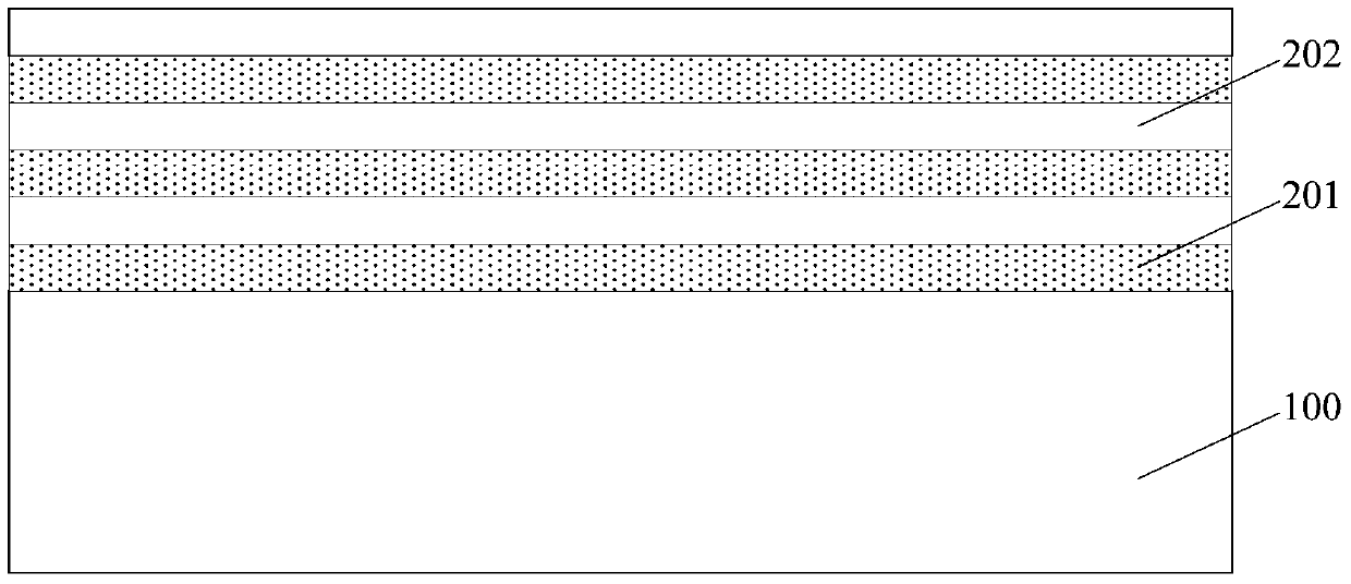
[0039] In an embodiment of the present invention, after the first semiconductor wire is formed, a second semiconductor layer is formed on the surface of the first semiconductor wire. The thickness of the second semiconductor layer is uniform, and as the channel layer of the field-effect transistor that fully surrounds the gate, compared with the gate structure directly formed on the first semiconductor line, the shape of the first semiconductor line has a greater impact on the performance of the transistor. The gate structure is formed on the surface of the second semiconductor layer, and the thickness of the second semiconductor layer is uniform, so that the performance of transistors formed at different positions will not be affected by the shape of the first semiconductor line.

[0040] In order to make the above objects, features an...


PUM


Abstract

A semiconductor structure and a forming method thereof are provided. The forming method comprises a substrate; a stack structure is formed on the surface of the substrate in order and comprises a plurality of sacrificial layers and a plurality of first semiconductor layers, the surface of the substrate is a sacrificial layer, and the sacrificial layers and the first semiconductor layers are stacked alternately; the stack structure is etched to form a groove in the surface of the substrate and a first semiconductor line and a sacrificial line on two sides of the groove; the sacrificial line is removed so that the first semiconductor line is suspended above the substrate; the first semiconductor line is subjected to annealing processing, so that the cross section of the first semiconductor line is round; an epitaxial technique is used to form a second semiconductor layer of the surface of the first semiconductor line, and the carrier mobility of the second semiconductor layer is greater than that of the first semiconductor nano line. The method can improve the performance of a fully surrounded gate field effect transistor formed on the first semiconductor nano line.

Description

technical field [0001] The invention relates to the technical field of semiconductors, in particular to a semiconductor structure and a forming method thereof. Background technique [0002] With the rapid development of semiconductor manufacturing technology, semiconductor devices are developing towards higher element density and higher integration. Transistors, as the most basic semiconductor devices, are currently being widely used. Therefore, as the component density and integration of semiconductor devices increase, the gate size of transistors is also getting shorter and shorter. However, the shortening of the gate size of the transistor will cause the short-channel effect of the transistor, thereby generating leakage current, and ultimately affecting the electrical performance of the semiconductor device. [0003] In order to overcome the short channel effect of the transistor and suppress the leakage current, a fully surrounded gate field effect transistor is propose...

Claims


Application Information

Patent Timeline
Patent Type & Authority Patents(China)
IPC IPC(8): H01L29/78H01L29/06H01L21/336
Inventor 禹国宾
Owner SEMICON MFG INT (SHANGHAI) CORP
Why Eureka
Try Eureka