

High-electron-mobility transistor device and manufacture method thereof
A technology with high electron mobility and manufacturing methods, applied in semiconductor/solid-state device manufacturing, transistors, semiconductor devices, etc., can solve the problems of easy failure of transistors, difficult heat dissipation, high temperature, etc., and achieve the effect of improving intermodulation distortion
- Summary
- Abstract
- Description
- Claims
- Application Information
AI Technical Summary
Problems solved by technology
Method used
Image

Examples
no. 1 approach
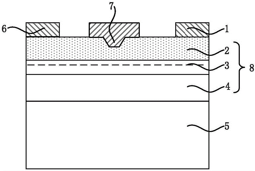
[0076] ginseng Figure 4G As shown, the high electron mobility transistor device in the first embodiment of the present invention includes a substrate 5, a semiconductor layer 8 formed on the substrate, and a source 6, a drain 1 and a gate formed on the semiconductor layer 8 7.
[0077] Wherein, the substrate 5 may be one or more of sapphire, silicon carbide, silicon, lithium niobate, silicon-on-insulator substrate, gallium nitride or aluminum nitride.
[0078] The semiconductor layer 8 sequentially includes from the direction of the substrate 5:
[0079] Buffer layer 4: not only plays the role of bonding the semiconductor material layer to be grown next, but also protects the substrate 5 from being invaded by some metal ions. In this embodiment, the buffer layer 4 is a gallium nitride layer (Al)GaN with a controllable aluminum content;
[0080] Channel layer 3: the channel layer 3 and the upper barrier layer 2 together form a heterojunction structure, and the channel layer...
no. 2 approach
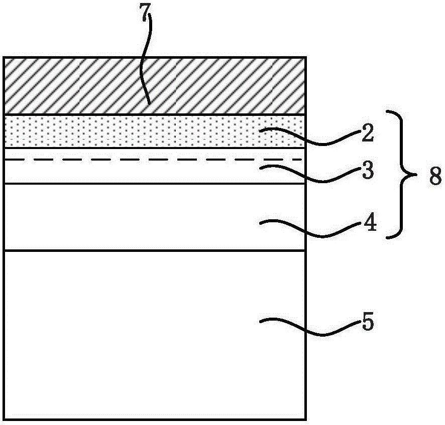
[0109] ginseng Figure 7E As shown, the high electron mobility transistor device in the second embodiment of the present invention also includes:
[0110] Substrate 5;
[0111] a buffer layer 4 on the substrate;
[0112] a channel layer 3 on the buffer layer;
[0113] a barrier layer 2 located on the channel layer;
[0114] The source 6 , the drain 1 and the gate 7 are located on the barrier layer, and the gate 7 is located between the source 6 and the drain 1 .
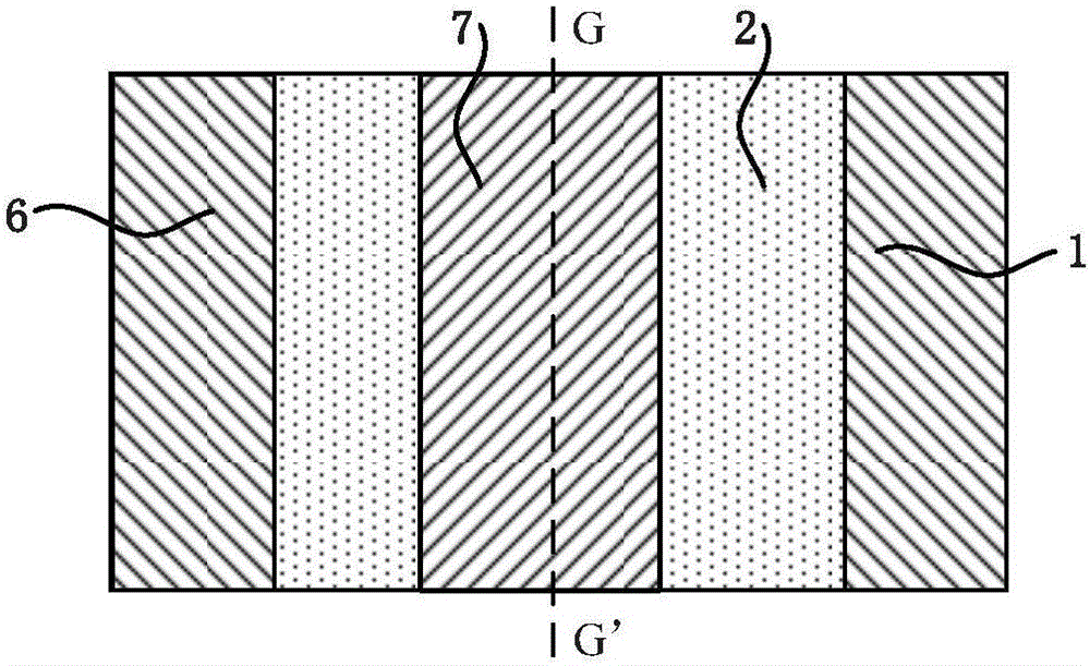
[0115] Different from the first embodiment, in this embodiment, there is no groove periodically changing along the gate width direction on the barrier layer 2 (see Figure 4E shown), but the gate region on the barrier layer is implanted with ions, so that the ion implantation dose changes periodically along the gate width direction (see Figure 7D shown).
[0116] Such as Figures 7A to 7E As shown, the manufacturing method in this embodiment includes the following steps:
[0117] S21: First, if Figure 7A A...
PUM
 Abstract
Description
Claims
Application Information