Programmable spinning logic device and electronic device employing same

A spin logic device and logic technology, applied in the field of spin electronics, can solve problems such as inconvenient manufacturing, high energy consumption of logic devices, and limitations on the practical application of spin logic devices, and achieve easy application, simple structure and operation Effect

Active Publication Date: 2016-08-24
INST OF PHYSICS - CHINESE ACAD OF SCI
View PDF3 Cites 13 Cited by
  • Summary
  • Abstract
  • Description
  • Claims
  • Application Information

AI Technical Summary

Problems solved by technology

First, it contains too much wiring, the structure is very complicated, and it is not easy to manufacture
Second, because it completely relies on the Oersted magnetic field generated by the current to flip the magnetization direction of the ferromagnetic layer, in order to generate a strong enough Oersted magnetic field to achieve the flip, a large current needs to be applied, thus resulting in energy consumption of the logic device very high
Third, the Oersted magnetic field generated by the current may affect the normal operation of the surrounding electronic devices. figure 1 A magnetic shield structure is formed around the logic device, which makes the structure more complicated and increases the cost
The above drawbacks limit the practical application of this state-of-the-art spin logic device

Method used


Image

  • Programmable spinning logic device and electronic device employing same
  • Programmable spinning logic device and electronic device employing same
  • Programmable spinning logic device and electronic device employing same

Examples


Embodiment Construction

[0033] Hereinafter, exemplary embodiments of the present invention will be described with reference to the drawings.

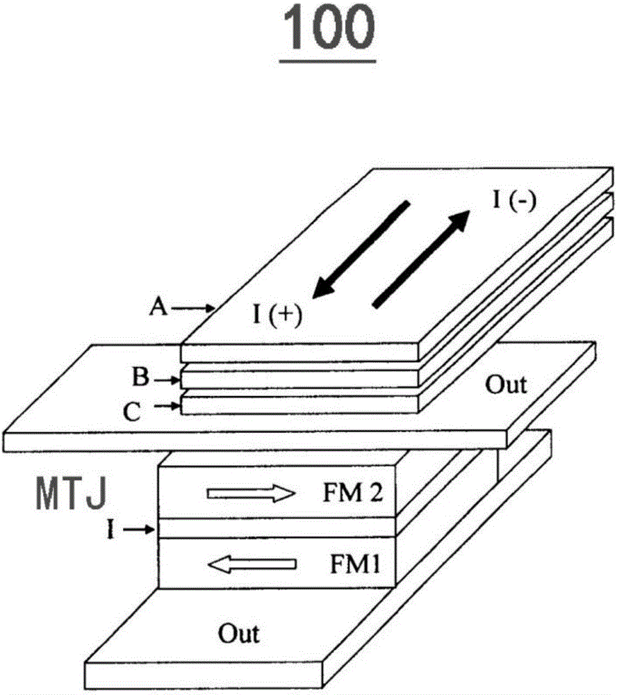
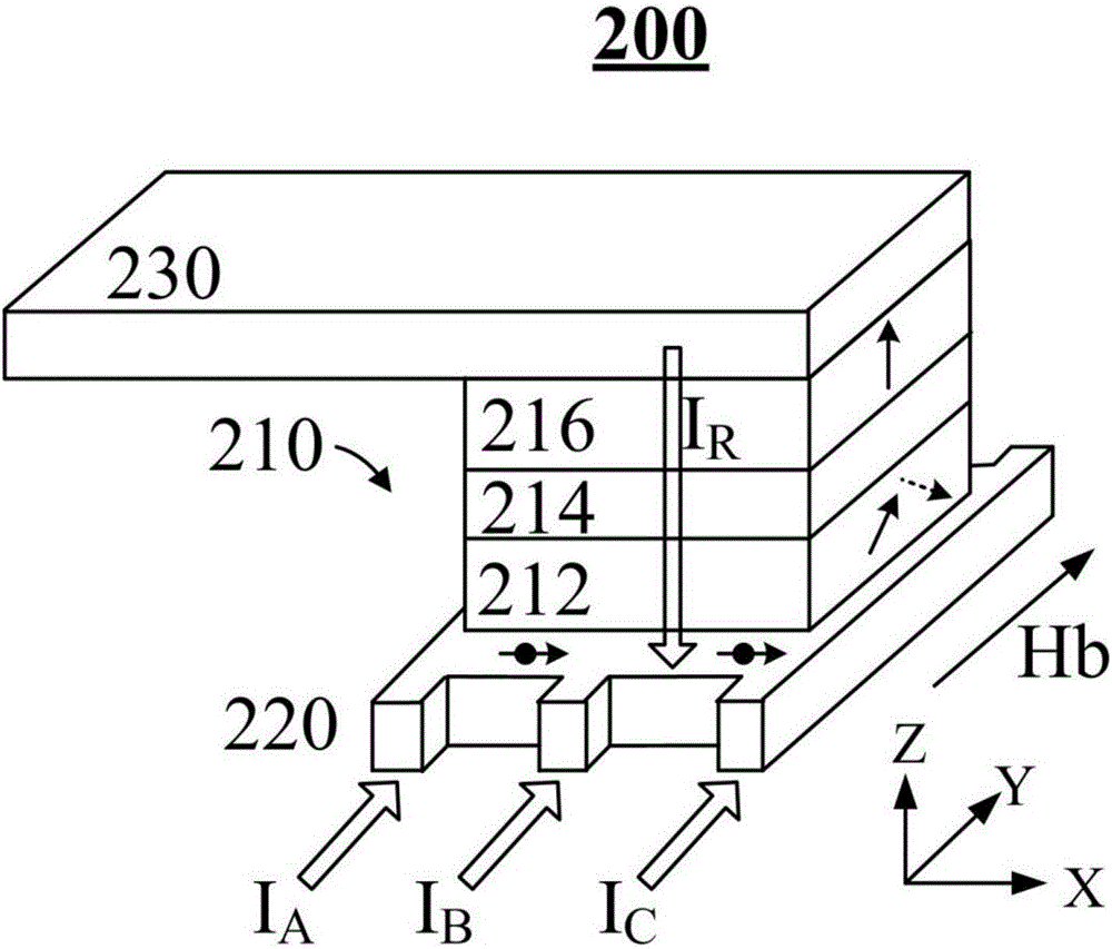
[0034] figure 2 A schematic structural diagram of a spin logic device 200 according to an embodiment of the present invention is shown. Such as figure 2 As shown, the spin logic device 200 includes a magnetic tunnel junction 210, a spin Hall effect (SHE) bias layer 220 located under the magnetic tunnel junction 210, and a current wiring 230 located above the magnetic tunnel junction 210.

[0035] Such as figure 2 As shown, the magnetic tunnel junction 210 may include a free magnetic layer 212, a reference magnetic layer 216, and a barrier layer 214 between the free magnetic layer 212 and the reference magnetic layer 216. Both the free magnetic layer 212 and the reference magnetic layer 216 may be formed of ferromagnetic materials, such as Co, Fe, Ni, and alloys including Co, Fe, and Ni, such as CoFe, NiFe, CoFeB, and the like. Wherein, the free magnetic layer 2...


PUM


Abstract

The invention relates to a programmable spinning logic device and an electronic device employing same. The programmable spinning logic device comprises an SHE bias layer formed by antiferromagnetic material with spin Hall effect, a magnetic tunnel junction including a free magnetic layer arranged on and contacted with the SHE bias layer, a barrier layer arranged on the free magnetic layer, and a referential magnetic layer arranged on the barrier layer, and electric wirings connect to one side of the referential magnetic layer of the magnetic tunnel junction to arrange the magnetic tunnel junction between the SHE bias layer and the electric wirings, wherein the SHE bias layer applies a bias magnetic field on the free magnetic layer along the first direction, and the SHE bias layer receives current in first, second and third surfaces. The direction of the current in the first and second surfaces is parallel to the first direction, and the current in the third surface controls the operation mode of the spinning logic device. The SHE bias layer and the electric wirings apply reading current flowing by the magnetic tunnel junction.

Description

Technical field [0001] The present invention generally relates to spintronics, and more particularly, to a pure current-driven programmable spin logic device that can operate under a zero magnetic field, and also relates to electronic equipment including the spin logic device. Background technique [0002] Digital logic devices designed using the electronic spin characteristics of magnetic materials are called spin logic devices or magnetic logic devices. Compared with ordinary semiconductor logic devices, this reconfigurable logic device based on spin-related transport characteristics has high operating frequency, unlimited reconfiguration times, non-volatility of logic information, radiation protection, and magnetic random storage. Taking advantage of memory (MRAM) compatibility and other advantages, it is considered a strong candidate for the next generation of logic devices to replace traditional semiconductor logic devices. [0003] figure 1 A spin logic device 100 in the pri...

Claims


Application Information

Patent Timeline
Patent Type & Authority Applications(China)
IPC IPC(8): H01L43/06H01L43/10H03K19/20
CPCH03K19/20H10N52/00H10N50/85
Inventor 韩秀峰张轩万蔡华
Owner INST OF PHYSICS - CHINESE ACAD OF SCI
Why Eureka
Try Eureka