A composite sensor and its manufacturing method
A composite sensor and manufacturing method technology, applied in the direction of manufacturing microstructure devices, piezoelectric devices/electrostrictive devices, piezoelectric/electrostrictive/magnetostrictive devices, etc., can solve unqualified products, difficult control, acceleration Reduced sensor detection accuracy and other issues, to achieve the effect of precise limit overload protection, simple structure, and easy production process
- Summary
- Abstract
- Description
- Claims
- Application Information
AI Technical Summary
Problems solved by technology
Method used
Image
Examples
Embodiment 1
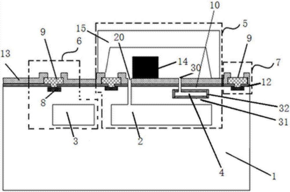
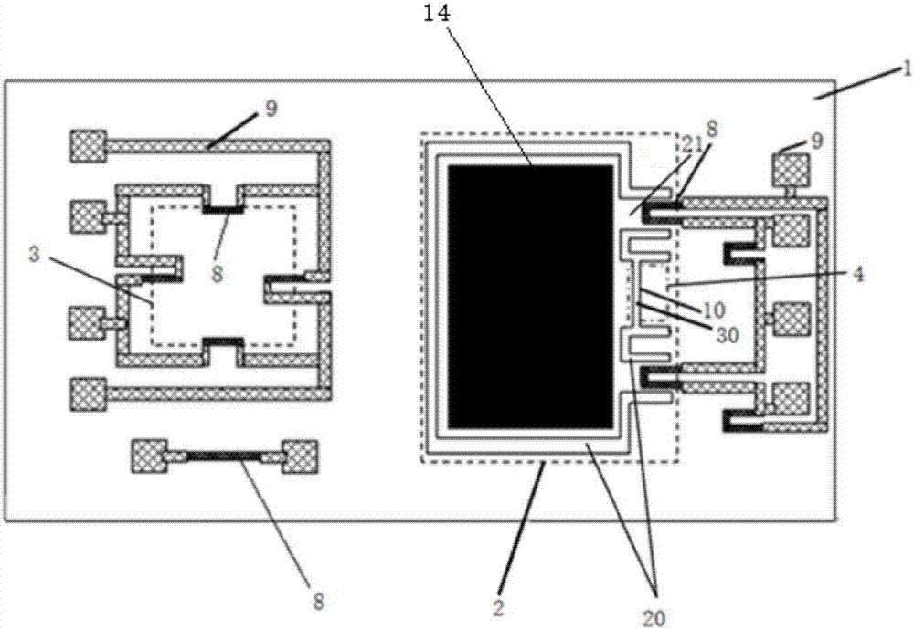
[0087] Such as figure 2 , image 3 As shown, a composite sensor, in which,
[0088] Silicon substrate 1, and a first predetermined cavity 2, a second predetermined cavity 3 formed in the silicon substrate 1, and a third predetermined cavity in the suspended silicon film above the first predetermined cavity 2 Cavity 4; wherein, preferably, the inner surface of the third predetermined cavity 4 may be provided with a second semiconductor mask layer 32 .
[0089] A plurality of semiconductor-doped resistors 8 for respectively forming an acceleration sensor 5, a pressure sensor 6, and a temperature sensor 7 are formed at predetermined positions on the surface of the silicon substrate 1, and the semiconductor-doped resistors 8 are electrically connected to the conductive wires 9;
[0090] Forming a first release groove 20 and a first connecting member 21 in the suspended silicon film above the first predetermined cavity 2, the first release groove 20 is arranged to avoid the semi...
Embodiment 2
[0100] A method of manufacturing a composite sensor, wherein,
[0101] providing a silicon substrate having at least one first pre-cavity and / or at least one second pre-cavity;
[0102] At least one third predetermined cavity is formed in the suspended silicon film in the at least one first prefabricated cavity; preferably, a second semiconductor mask layer is formed on the inner surface of the at least one third predetermined cavity.
[0103] Several semiconductor-doped resistors for forming pressure sensors, acceleration sensors, and temperature sensors are formed above the silicon substrate, and the semiconductor-doped resistors are electrically connected to conductive wires;
[0104] forming a first connection member and a first release groove in the suspended silicon film above the at least one first predetermined cavity, the first release groove avoids the semiconductor doping resistance arrangement,
[0105] The suspended silicon film above the at least one third prede...
specific Embodiment approach
[0114] Such as Figures 4A-4B , Figure 15 As shown, in step S1, the silicon substrate 100 is provided, and the first prefabricated cavity 101 and the second prefabricated cavity 102 for forming the suspended release structure are fabricated on the silicon substrate; the movable structure of the acceleration sensor is located at The upper end of the first prefabricated cavity, the movable structure of the acceleration sensor includes a first connecting member and a mass block, and the first prefabricated cavity 101 and the second prefabricated cavity 102 are independent of each other. The height of the first prefabricated cavity 101 is h1, and the height h1 of the first prefabricated cavity 101 is used to limit the distance of the vertical movement of the mass, especially the vertical downward movement of the mass (that is, the limit in the -Z direction), The height h1 of the first prefabricated cavity 101 can also be used to adjust air damping and improve the dynamic performan...
PUM
| Property | Measurement | Unit |
|---|---|---|
| thickness | aaaaa | aaaaa |
Abstract
Description
Claims
Application Information


