Composite sensor and production method

A composite sensor and manufacturing method technology, applied in the direction of manufacturing microstructure devices, piezoelectric devices/electrostrictive devices, piezoelectric/electrostrictive/magnetostrictive devices, etc., can solve unqualified products, difficult control, acceleration Reduced sensor detection accuracy and other issues, to achieve the effect of precise limit overload protection, simple structure, and easy production process

Active Publication Date: 2016-08-31
GUANGDONG HEWEI INTEGRATED CIRCUIT TECH
View PDF8 Cites 6 Cited by
  • Summary
  • Abstract
  • Description
  • Claims
  • Application Information

AI Technical Summary

Problems solved by technology

[0004] The disadvantage of the above technical solution is that the overload protection of the acceleration sensor part depends on the prefabricated buried cavity depth c 1 and the distance from the protective cap to the top layer of the accelerometer mass block c 2 to fulfill
Usually buried cavity depth c 1 Formed by etching, and then the buried cavity depth c can be controlled during the fabrication process 1 ; while c 2 It is relatively difficult to control, because c 2 not only as deep as the cavity inside the cap c 3 It is also related to the mass block thickness c on the acceleration sensor 4 It is related, and usually the quality block is

Method used


Image

  • Composite sensor and production method
  • Composite sensor and production method
  • Composite sensor and production method

Examples


Embodiment 1

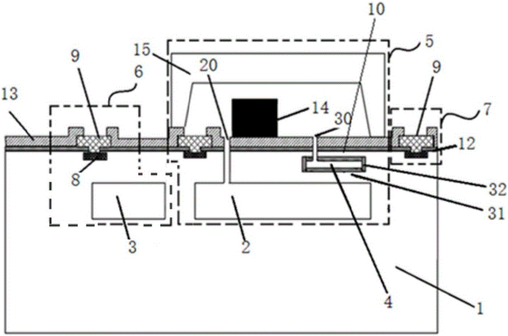
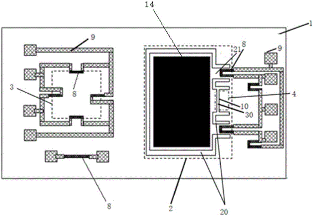
[0087] Such as figure 2 , image 3 As shown, a composite sensor, in which,

[0088] Silicon substrate 1, and a first predetermined cavity 2, a second predetermined cavity 3 formed in the silicon substrate 1, and a third predetermined cavity in the suspended silicon film above the first predetermined cavity 2 Cavity 4; wherein, preferably, the inner surface of the third predetermined cavity 4 may be provided with a second semiconductor mask layer 32 .

[0089] A plurality of semiconductor-doped resistors 8 for respectively forming an acceleration sensor 5, a pressure sensor 6, and a temperature sensor 7 are formed at predetermined positions on the surface of the silicon substrate 1, and the semiconductor-doped resistors 8 are electrically connected to the conductive wires 9;

[0090] Forming a first release groove 20 and a first connecting member 21 in the suspended silicon film above the first predetermined cavity 2, the first release groove 20 is arranged to avoid the semi...

Embodiment 2

[0101] A method of manufacturing a composite sensor, wherein,

[0102] providing a silicon substrate having at least one first pre-cavity and / or at least one second pre-cavity;

[0103] At least one third predetermined cavity is formed in the suspended silicon film in the at least one first prefabricated cavity; preferably, a second semiconductor mask layer is formed on the inner surface of the at least one third predetermined cavity.

[0104] Several semiconductor-doped resistors for forming pressure sensors, acceleration sensors, and temperature sensors are formed above the silicon substrate, and the semiconductor-doped resistors are electrically connected to conductive wires;

[0105] forming a first connection member and a first release groove in the suspended silicon film above the at least one first predetermined cavity, the first release groove avoids the semiconductor doping resistance arrangement,

[0106] The suspended silicon film above the at least one third prede...

specific Embodiment approach

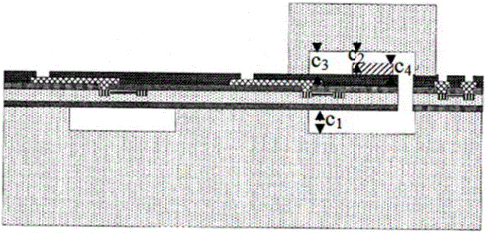
[0115] Such as Figures 4A-4B , Figure 15 As shown, in step S1, the silicon substrate 100 is provided, and the first prefabricated cavity 101 and the second prefabricated cavity 102 for forming the suspended release structure are fabricated on the silicon substrate; the movable structure of the acceleration sensor is located at The upper end of the first prefabricated cavity, the movable structure of the acceleration sensor includes a first connecting member and a mass block, and the first prefabricated cavity 101 and the second prefabricated cavity 102 are independent of each other. The height of the first prefabricated cavity 101 is h1, and the height h1 of the first prefabricated cavity 101 is used to limit the distance of the vertical movement of the mass, especially the vertical downward movement of the mass (that is, the limit in the -Z direction), The height h1 of the first prefabricated cavity 101 can also be used to adjust air damping and improve the dynamic performan...


PUM

PropertyMeasurementUnit
Thicknessaaaaaaaaaa

Abstract

The invention relates to the technical field of sensor processing, and especially relates to a composite sensor and a production method. The composite sensor comprises a silicon substrate, and at least one first preset cavity, at least one second preset cavity and at least one third preset cavity in the silicon substrate. A plurality of semiconductor doped resistors for forming an acceleration sensor, a pressure sensor and a temperature sensor are formed at preset positions on the surface of the silicon substrate. The semiconductor doped resistors are electrically connected with conductive wires. A first release slot is formed on suspended silicon film at the upper side of the at least one first preset cavity. A second release slot is formed on suspended silicon film at the upper side of the at least one third preset cavity. The first release slot is combined with the second release slot, thus forming a suspended release structure. A limiting baffle plate is arranged out of the movable structure of the acceleration sensor. The limiting baffle plate has precise overload limiting protection effect. Moreover, an overload limiting device is simple in structure. The production process is relatively easy to grasp. The batch production of the product can be realized.

Description

technical field [0001] The invention relates to the technical field of sensor processing, in particular to a composite sensor based on MEMS processing technology and a manufacturing method. Background technique [0002] With the continuous development of MEMS technology and the maturity of silicon micromachining process, the composite sensor integrating silicon micromachining acceleration sensor, pressure sensor and temperature sensor is widely used because of its low price, high precision and suitable for mass production. . [0003] The Chinese invention patent with application number CN104058361A discloses a processing method for an integrated piezoresistive accelerometer and pressure gauge based on a prefabricated cavity SOI substrate, such as figure 1 As shown, the accelerometer includes a base made of silicon, a cantilever beam made of silicon, a sensitive mass made of silicon, a force sensitive resistor made of silicon, and metal leads. The pressure gauge includes a ...

Claims


Application Information

Patent Timeline
IPC IPC(8): B81C1/00B81B3/00
CPCB81B3/0064B81C1/00015
Inventor 朱二辉周志健陈磊杨力建邝国华
Owner GUANGDONG HEWEI INTEGRATED CIRCUIT TECH
Why Eureka
Try Eureka