
Multilayer ceramic electronic device

A technology for electronic components and ceramics, which is applied in the field of laminated ceramic electronic components, can solve the problem of not establishing cracks, etc., and achieve the effects of less reduction in electrostatic capacitance and suppression of cracks.

Active Publication Date: 2016-10-12
TDK CORPARATION
View PDF6 Cites 9 Cited by
  • Summary
  • Abstract
  • Description
  • Claims
  • Application Information

AI Technical Summary

Problems solved by technology

Until now, in the case of reducing the thickness of the dielectric layer to 0.5 μm or less, and further reducing the thickness to 0.4 μm or less, no technical means have been established to prevent the occurrence of cracks and ensure the electrostatic capacity.

Method used


Image

  • Multilayer ceramic electronic device
  • Multilayer ceramic electronic device
  • Multilayer ceramic electronic device

Examples


Embodiment 1

[0086] First, as the raw material powder of the main raw material, {(Ba 1-x-y Ca x Sr y )O} u (Ti 1-z Zr z ) v o 3 powder (x=0.05, y=0, z=0.05, u / v=1.004), then prepare MgCO 3 , MnCO 3 , Y 2 o 3 , SiO 2 as a side ingredient. In addition, the subcomponents are preliminarily crushed and processed to a particle diameter of about 40 nm smaller than that of the barium titanate raw material.

[0087] Next, 0.5 mol of MgCO was weighed for each raw material powder prepared above with respect to 100 mol of the main raw material. 3 powder, 0.3 mol MnCO 3 powder, 0.2 mole of Y 2 o 3 powder and weigh 2 moles of SiO 2 powder. These respective powders were wet-mixed with a ball mill and dried for 20 hours to obtain a dielectric raw material for the capacitor part. BaCO added at this time 3 , MnCO 3 After firing, they are contained in the dielectric ceramic composition as BaO and MnO, respectively.

[0088] Next, the obtained dielectric raw material: 100 parts by weight,...

Embodiment 2

[0110] As shown in Table 2, except that the thickness td of the dielectric layer 10 after firing and the thickness te of the internal electrode layer 12 after firing were set to 0.3 μm, samples of laminated ceramic capacitors were produced in the same manner as in Example 1, and measured Their electrostatic capacitance and crack generation rate. The results are shown in Table 2.

[0111] [Table 2]

[0112]

[0113] Evaluation 1

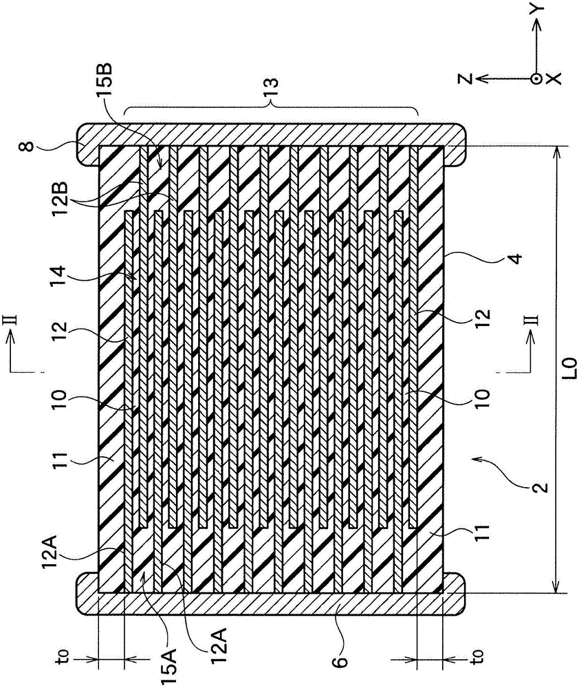
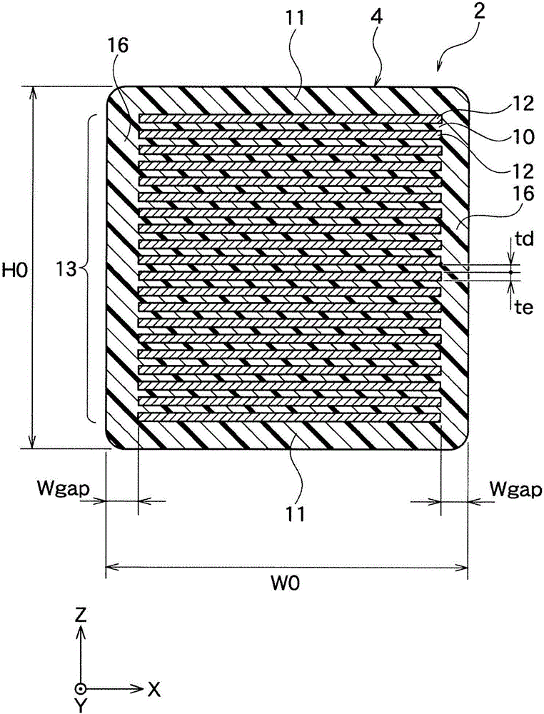
[0114] From the results shown in Table 1 and Table 2, it can be confirmed that the thickness td of the dielectric layer is 0.4 μm or less, the width dimension W0 is 0.59 mm or less, the gap dimension Wgap is 0.010 to 0.025 mm, and the ratio (Wgap / W0 dimension) is 0.025 or more, a multilayer ceramic capacitor with a low crack occurrence rate and a small decrease in capacitance.

Embodiment 3

[0116] As shown in Table 3, except that the thickness te of the internal electrode layer 12 after firing was changed, samples of multilayer ceramic capacitors were produced in the same manner as in Example 1, and their capacitances and crack occurrence rates were measured. The results are shown in Table 3.

[0117] [table 3]

[0118]

[0119] Evaluation 2

[0120] From the results shown in Table 3, it was confirmed that when te / td is less than 1.25, and particularly preferably te / td is 0.95 to 1.05, a multilayer ceramic capacitor with a low rate of occurrence of cracks and a small decrease in capacitance can be obtained.


PUM

PropertyMeasurementUnit
Thicknessaaaaaaaaaa
Gap sizeaaaaaaaaaa
Width sizeaaaaaaaaaa

Abstract

A multilayer ceramic electronic device comprising: a ceramic element body, in which a plurality of dielectric layers and a plurality of internal electrode layers are alternately stacked, and at least a pair of external electrodes which are connected to the internal electrode layers on surfaces of the ceramic element body; a thickness of the dielectric layers is 0.4 [mu]m or less, a width (W0) of the ceramic element body along a width-direction is 0.59 mm or less, a gap (Wgap) between an outer face of the ceramic element body and an end of the internal electrode layers along width-direction of the ceramic element body is 0.010 to 0.025 mm, and a ratio (Wgap / W0) of the gap with respect to the width is 0.025 or more.

Description

technical field [0001] The present invention relates to a laminated ceramic electronic component having an extremely thin dielectric layer. Background technique [0002] Miniaturization and thinning of electronic equipment are sought, and miniaturization and thinning of laminated ceramic electronic components housed therein are also sought. Accordingly, thinning of dielectric layers in laminated ceramic electronic components is sought. [0003] For example, as shown in Patent Document 1, it is known that if the dielectric layer in a laminated ceramic electronic component is thinned, cracks will occur during its manufacture, and a method for preventing the cracks is disclosed. [0004] However, conventionally, the limit of the thickness of the dielectric layer is about 1 μm, however, according to recent technological innovations, a technique for reducing the thickness of the dielectric layer to 0.5 μm or less has been disclosed. Conventionally, when the thickness of the die...

Claims


Application Information

Patent Timeline
IPC IPC(8): H01G4/12H01G4/30
CPCH01G4/12H01G4/30H01G4/1209H01G4/1227H01G4/232H01G4/012
Inventor 室泽尚吾兼子俊彦
Owner TDK CORPARATION
Learn More