High-voltage power device terminal structure

A high-voltage power device and terminal structure technology, which is applied to semiconductor devices, electrical components, circuits, etc., can solve the problem of high peak value of the surface electric field in the terminal area, and achieve the effect of avoiding premature breakdown

Inactive Publication Date: 2016-10-12
UNIV OF ELECTRONICS SCI & TECH OF CHINA
View PDF5 Cites 12 Cited by
  • Summary
  • Abstract
  • Description
  • Claims
  • Application Information

AI Technical Summary

Problems solved by technology

[0004] The purpose of the present invention is to solve the problem that the peak value of the surface electric field in the terminal area is high in the reverse blocking state of the semiconductor power device in the high-voltage field, and propose a high-voltage power device terminal structure with a low surface electric field to avoid the occurrence of breakdown points on the semiconductor surface

Method used


Image

  • High-voltage power device terminal structure
  • High-voltage power device terminal structure
  • High-voltage power device terminal structure

Examples


Embodiment 1

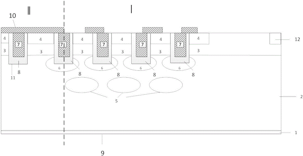
[0018] Such as figure 1 As shown, this example includes a device transition termination region and a device termination; the cathode electrode 9, a heavily doped single crystal silicon substrate 1, and an N-doped region 2 are sequentially stacked from bottom to top in the device transition termination region and device termination and N-type region 3; the upper layer of the N-type region 3 of the device transition termination region and the N-type region 3 of part of the device termination has a P-type heavily doped region 4; there is a first trench 11 in the device transition termination region, the first The trench 11 vertically and downwardly runs through the P-type heavily doped region 4 and the N-type region 3 along the upper surface of the transition terminal region of the device and extends into the N-doped region 2; the first trench 11 is filled with a dielectric 8 , there is polysilicon 7 in the medium 8, the upper surface of the P-type heavily doped region 4 of the d...

Embodiment 2

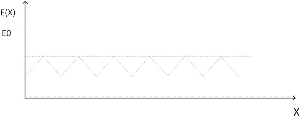
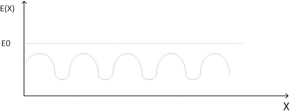
[0024] Such as Figure 4 As shown, the structure of this example is based on Example 1, and the floating island structure is used as a multi-layer, which can further reduce the peak value of the electric field on both sides of the P-type guard ring of the terminal structure.

[0025] Taking Example 1 as an example, a terminal structure of a high-voltage power device with a low surface electric field of the present invention can be prepared by the following method, and the process steps are:

[0026] 1. Monocrystalline silicon preparation. An N-type heavily doped single crystal silicon substrate 2 is used, and the crystal orientation is .

[0027] 2. Epitaxial growth. An N-type epitaxial layer with a certain thickness and doping concentration is grown by methods such as vapor phase epitaxy (VPE).

[0028] 3. The floating P-type island 5 is injected. Such as Figure 7 As shown, the pattern of the floating P-type island 5 is carved, and then high-energy boron ion implantatio...


PUM


Abstract

The invention belongs to semiconductor technology, and specifically relates to a high-voltage power device terminal structure. The high-voltage power device terminal structure comprises a groove in a silicon chip body and P-type protective rings, combination of the internal groove and the protective rings allows the peak value of an electric field to be transferred from the surface of the silicon chip into the body, and the breakdown points of a terminal area are transferred from the surface of the silicon chip to the two sides of a dielectric layer in the groove. Since the critical breakdown electric field (about 1e7V / cm) of the dielectric layer is far higher than a critical breakdown electric field (about 1e5V / cm) of silicone, P-type floating islands in staggered arrangement with the P-type protective rings reduce the peak values of the electric fields on the two sides of the P-type protective rings without reducing the reverse blockout voltage of a terminal area, thereby preventing premature breakdown of PN junctions in the silicon chip body.

Description

technical field [0001] The invention belongs to semiconductor technology, in particular to a terminal structure of a high-voltage power device. Background technique [0002] High-voltage power semiconductor devices have been widely used in the field of power supply in recent years. For example, IGBT (insulated gate bipolar transistor), FRD (fast recovery diode) are used in automotive drive, induction heating and other fields, and high-voltage MOSFET is used in LLC (logic chain road control) topology. In order to improve the performance of high-voltage power devices, researchers at home and abroad have successively proposed various structures, such as super-junction structures, trench MOS combined with P-type guard ring structures, and so on. These structures are used to increase the doping concentration of the N-drift region to reduce the forward conduction resistance of the MOSFET. [0003] An important issue to be considered in the design of high-voltage power devices is...

Claims


Application Information

Patent Timeline
Patent Type & Authority Applications(China)
IPC IPC(8): H01L29/06H01L29/78
CPCH01L29/0615H01L29/7833
Inventor 李泽宏李爽陈文梅陈哲曹晓峰李家驹罗蕾任敏
Owner UNIV OF ELECTRONICS SCI & TECH OF CHINA
Why Eureka
Try Eureka