Photomultiplier organic light detector with spectral selectivity and preparation method of photomultiplier organic light detector
A photoelectric multiplication and photodetector technology, applied in the field of photodetection, can solve the problems of device performance degradation, no coverage band, increased manufacturing cost of organic photodetectors, and application complexity, etc., and achieves economical and simple preparation methods, device The effect of simple structure
- Summary
- Abstract
- Description
- Claims
- Application Information
AI Technical Summary
Problems solved by technology
Method used
Image
Examples
Embodiment 1
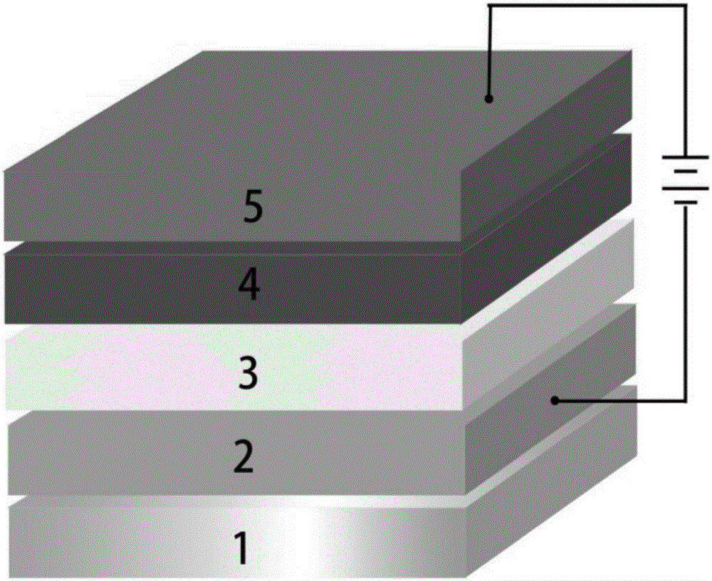
[0054] The photomultiplier organic photodetector with spectral selectivity comprises: a transparent substrate 1 , a transparent electrode 2 , a transparent electrode modification layer 3 , an active layer 4 and a metal electrode 5 .
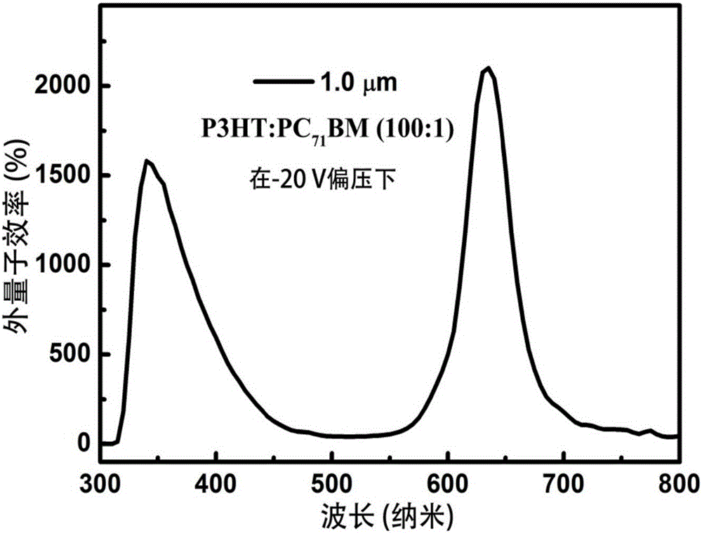
[0055] The transparent electrode 2 is a transparent ITO electrode; the transparent electrode modification layer 3 is poly(3,4-ethylenedioxythiophene)-polystyrenesulfonic acid (PEDOT:PSS); the active layer 4 is poly The blend film of (3-hexylthiophene) P3HT and fullerene derivative PCBM, wherein, the mass ratio of poly(3-hexylthiophene) P3HT and fullerene derivative PCBM is 100:1, and the thickness of active layer 4 is 2.0 μm; the metal electrode 5 is aluminum.
[0056] The preparation method of the above-mentioned organic photodetector comprises the following steps:
[0057] Step 1: Divide the area to 4cm 2 Glass serves as a transparent substrate.
[0058] Step 2: Plating indium tin oxide (ITO) on the transparent substrate, then soaking in dei...
Embodiment 2
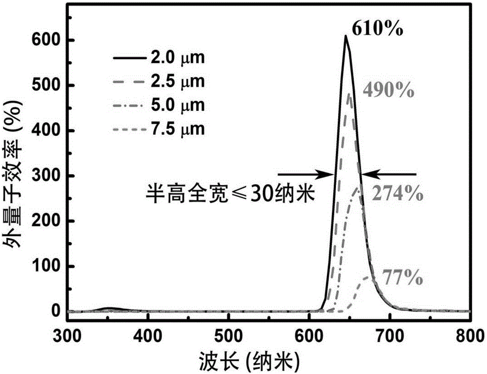
[0065] The thickness of the blended film of the active layer 4 in Example 1 is set to 2.5 μm and 5.0 μm respectively, such as image 3 As shown, the external quantum efficiencies of the organic photodetectors in both cases are greater than 100%, and the full width at half maximum (FWHM) are both less than 30nm, and both have spectral selectivity.
[0066] Apparently, the above-mentioned embodiments of the present invention are only examples for clearly illustrating the present invention, and are not intended to limit the implementation of the present invention. Those of ordinary skill in the art can also make There are other different forms of changes or changes, such as the preparation of the active layer, there are many options, and the electron donor material can be any one of poly(3-hexylthiophene) (P3HT) and perylene polymer (PBDT-TS1) The electron acceptor material can be any one of fullerene derivatives (PCBM, ICBA) or non-fullerene acceptors (ITIC), and it is impossibl...
PUM
| Property | Measurement | Unit |
|---|---|---|
| Thickness | aaaaa | aaaaa |
| Thickness | aaaaa | aaaaa |
| Thickness | aaaaa | aaaaa |
Abstract
Description
Claims
Application Information


