Scintillator device regulated and controlled by plasmon crystal
A plasmon and scintillator technology, which is applied in the field of nuclear radiation detection, can solve the problems of inability to regulate the luminescence decay time of scintillators, inability to regulate the directionality of luminescence, etc., and achieves the effect of improving detection efficiency and mature preparation technology.
- Summary
- Abstract
- Description
- Claims
- Application Information
AI Technical Summary
Problems solved by technology
Method used
Image
Examples
Embodiment 1
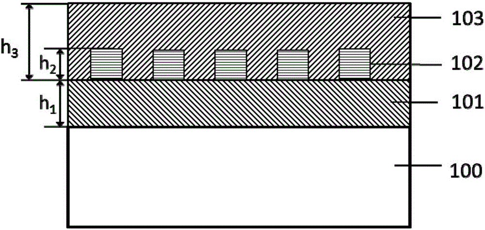
[0032] The structural parameters are selected as follows: the metal periodic structure is a triangular structure. Period a=300nm, d=0.4X300nm=120nm, h 1 =40nm,h 2 =40nm, h 3 = h 1 + h 2 = 80nm.
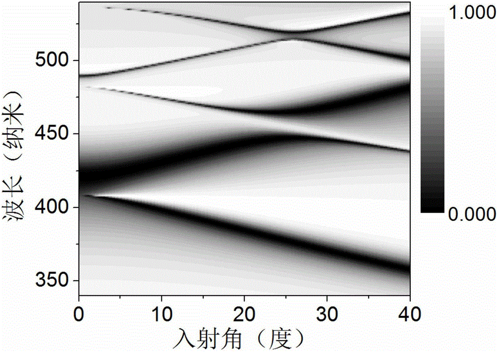
[0033] In order to illustrate that the structure has a significant luminescence control effect in the normal direction, we performed FDTD simulations on the dispersion relationship of the optical properties of the structure, as shown in figure 2 shown. The results show that in the wavelength range of 400-420nm, the optical modes for the optical modes are mainly concentrated near 0 degrees, that is, near the normal direction.
[0034] The preparation process is as follows:
[0035] A first scintillator layer is prepared on a quartz substrate. A certain amount of Lu(NO 3 ) 3 6H2O (99.99%), Ce (NO 3 ) 3 ·6H 2O was dissolved in 2-methylethanol (99.99%, AR), ultrasonicated and stirred at room temperature until it was completely dissolved and became transparent, and then tetra...
Embodiment 2
[0041] A scintillator device regulated by plasmonic crystals, comprising a base layer, a first scintillator layer arranged on the base layer, a metal periodic array layer arranged on the first scintillator layer, and a metal periodic array layer arranged on the metal periodic array layer The metal periodic array layer in the above structure is actually immersed in the middle of the scintillator layer, but the preparation process must first prepare the first scintillator layer, then prepare the metal periodic array layer, and then prepare the second scintillator layer. The first scintillator layer is firmly in contact with the base layer and has sufficient hardness to bear the force during the preparation process of the metal periodic array layer.
[0042] The base layer is a silicon wafer with a flat surface. The metal periodic array layer is composed of columnar metal units distributed periodically in a square structure. The material of the metal units is silver, and the dist...
Embodiment 3
[0048] A scintillator device regulated by plasmonic crystals, the structure of which is basically the same as that of Embodiment 2, except that the substrate is quartz glass with a flat surface, and the metal periodic array layer is composed of columnar metal units periodically distributed in a triangular structure , the material of the metal unit is aluminum, the distance between adjacent metal units is 300nm, the diameter of the metal unit is 0.4 of the distance between adjacent metal units, and the height of the metal unit is 50nm.
[0049] The composition of the first scintillator layer is Lu 2 SiO 5 : Ce, with a thickness of 40nm, is produced by sol-gel method, and the temperature of the burning process is 1200°C, which is an optimal crystallization temperature and can obtain the optimal luminous efficiency. The composition of the second scintillator layer is Lu 2 SiO 5 : Ce, the thickness is the sum of the height of the first scintillator layer and the height of the m...
PUM
| Property | Measurement | Unit |
|---|---|---|
| Thickness | aaaaa | aaaaa |
| Thickness | aaaaa | aaaaa |
| Thickness | aaaaa | aaaaa |
Abstract
Description
Claims
Application Information


