Transconductance amplifier with low noise and high output resistance

A transconductance amplifier and high output technology, applied in the field of transconductance amplifier, can solve the problems of limited voltage amplification capability, low output resistance, instability, etc., and achieve the effect of reducing power consumption

Active Publication Date: 2016-10-26
深圳市时代速信科技有限公司
View PDF3 Cites 11 Cited by
  • Summary
  • Abstract
  • Description
  • Claims
  • Application Information

AI Technical Summary

Problems solved by technology

Each of these structures has advantages and disadvantages: CS structure see figure 1 , it has a certain transconductance and the lowest noise, but in the deep submicron CMOS process, the output resistance introduced by channel length modulation is very low, which limits its voltage amplification capability; the Cascode structure see figure 2 , which consists of stacked common-source and common-gate transistors, L m It is used to tune out the parasitic capacitance of the intermediate node. Compared with CS, the output resistance of Cascode is much higher, and its transconductance can be close to the transconductance of CS structure under the action of gate feedback

Method used


Image

  • Transconductance amplifier with low noise and high output resistance
  • Transconductance amplifier with low noise and high output resistance
  • Transconductance amplifier with low noise and high output resistance

Examples


Embodiment Construction

[0019] Achieving optimum performance of the transconductance amplifier of the present invention requires careful selection of parameter values ​​for each element.

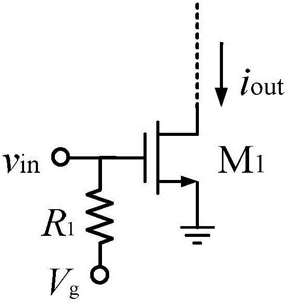
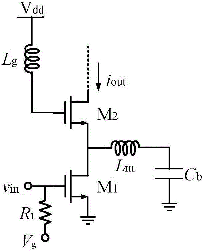
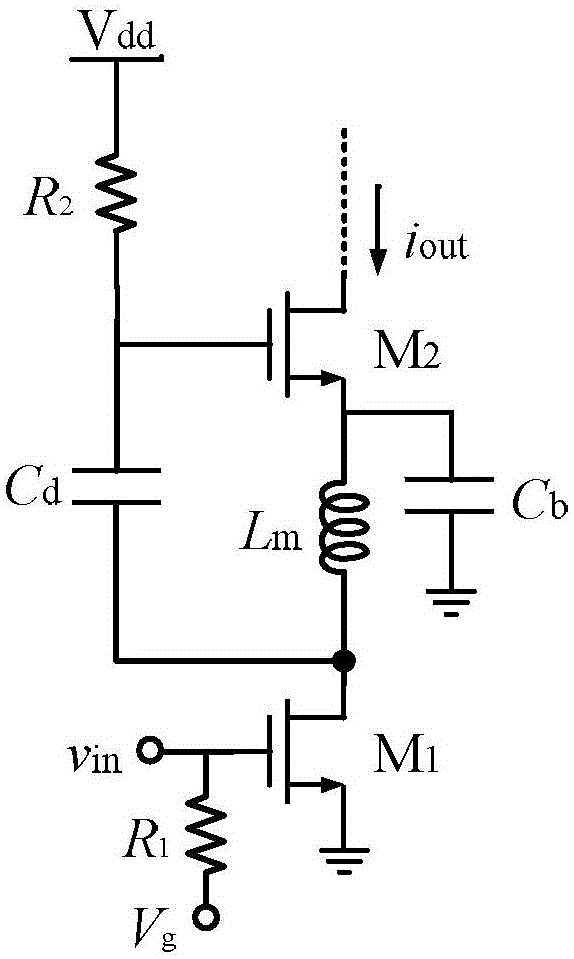
[0020] see Figure 4 , the low-power, low-noise and high-gain transconductance amplifier of the present invention is provided with a common source transistor M 1 , positive feedback transistor M 2 , output transistor M 3 , Interstage tuning inductance L m , gate feedback inductance L g , DC blocking capacitor C d , Bypass capacitor C b with the bias resistor R 1 and R 2 . Among them, the blocking capacitor C d with bypass capacitor C b Both self-resonances are at the operating frequency, and they can be ignored in AC analysis; the bias resistor R 1 and R 2 Used to prevent the flow of AC signals, its typical value is in the order of 10K ohms. Input signal with M 1 connected to the gate, M 1 The source is grounded and its DC bias voltage is passed through R 1 added to its gate, M 1 the drain simultan...


PUM


Abstract

The invention discloses a transconductance amplifier with low noise and a high output resistance. The transconductance amplifier is provided with a transistor M1, a transistor M2, a transistor M3, an inductor Lm, an inductor Lg, a capacitor Cd, a capacitor Cb, a resistor R1 and a resistor R2. An input signal is connected with the grid of the M1; the source of the M1 is grounded; a bias is added to the grid of the M1 via the R1; the drain of the M1 is connected with the source of the M3, one end of the Cd and one end of the Lm; the other end of the Cd and the other end of the Lm are connected with the grid and the source of the M2, respectively; the source of the M2 is connected with one end of the Cb, while the other end of the Cb is grounded; the R2 is arranged between a Vdd and the grid of the M2; the Lg is arranged between the source of the M2 and the Vdd; the drain of the M2 is connected with the grid of the M3; and the drain of the M3 is a current output end. As feedback is introduced, the voltage between the grid and source of the M3 is enhanced, the equivalent transconductance is improved, the output resistance is increased, and the noise brought by the M3 is inhibited. The transconductance amplifier has the characteristics of high transconductance and output resistance and low noise, and is applicable to the application occasions such as a millimeter wave low noise amplifier.

Description

technical field [0001] The invention relates to an amplifier in a millimeter wave circuit, in particular to a transconductance amplifier with low noise and high output resistance. The CMOS technology is adopted, which has great advantages in the millimeter wave circuit, and the design structure is simple, so that the amplifier can obtain low noise and high output resistance at the same time. High-gain characteristics, while having the same noise and gain performance as conventional amplifiers, can greatly reduce the power consumption of the amplifier. Background technique [0002] In a millimeter-wave low-noise amplifier, on the one hand, it is hoped that its own noise figure is as low as possible to minimize the noise contribution to the receiving chain, and on the other hand, it is also hoped that it has a high gain to suppress the noise effect of the subsequent circuit. The voltage gain of the amplifier can be represented by the product of the transconductance and the out...

Claims


Application Information

Patent Timeline
IPC IPC(8): H03F1/26
CPCH03F1/26
Inventor 李智群王冲李芹王志功
Owner 深圳市时代速信科技有限公司
Why Eureka
Try Eureka