Micro-lattice mismatch quantum well solar cell and manufacturing method therefor

A technology of solar cells and quantum wells, applied in the field of solar cells, can solve problems such as difficult control of cell defects

Active Publication Date: 2016-11-02
ZHONGSHAN DEHUA CHIP TECH CO LTD
View PDF10 Cites 15 Cited by
  • Summary
  • Abstract
  • Description
  • Claims
  • Application Information

AI Technical Summary

Problems solved by technology

[0008] The cell defects of the large lattice mismatch structure with high In composition are not easy to control, and the simple quantum well structure will cause a large drop in open circuit voltage due to the low band gap of the potential well layer. Therefore, this patent proposes a microlattice A m

Method used


Image

  • Micro-lattice mismatch quantum well solar cell and manufacturing method therefor
  • Micro-lattice mismatch quantum well solar cell and manufacturing method therefor
  • Micro-lattice mismatch quantum well solar cell and manufacturing method therefor

Examples


Embodiment Construction

[0048] The present invention will be further described below in conjunction with specific examples.

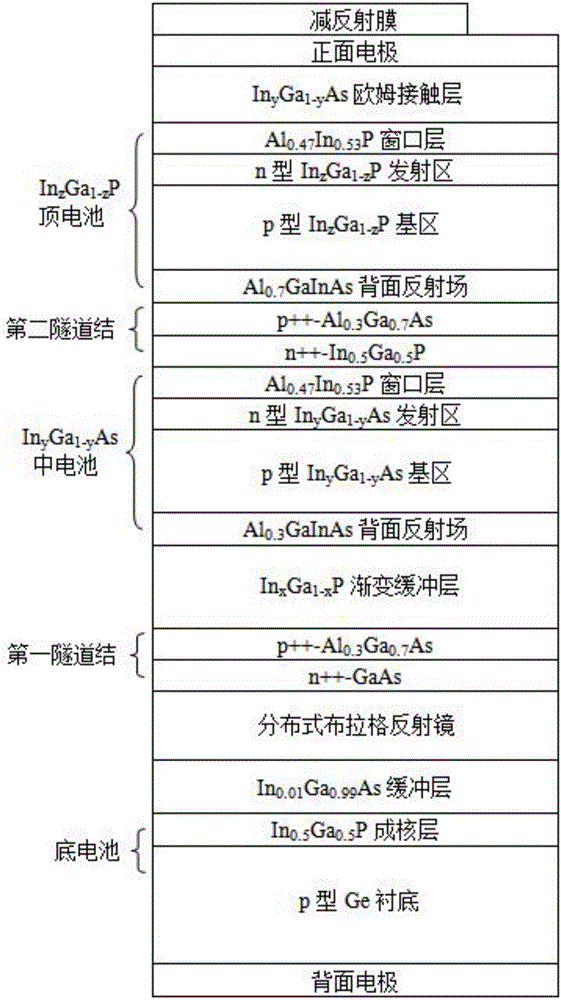
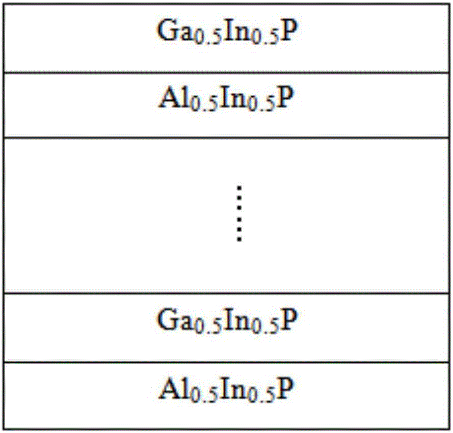
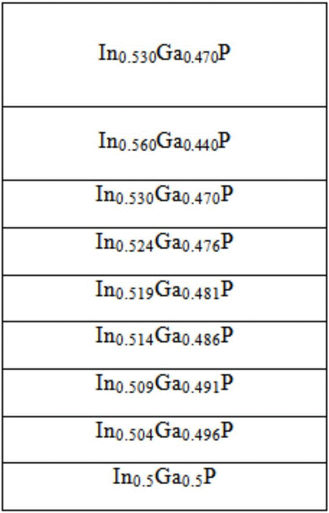
[0049] Such as figure 1 As shown, the microlattice mismatch quantum well solar cell described in this embodiment is mainly composed of "Ge / In y Ga 1- y As / In z Ga 1-z P" triple junction structure, can also be "Ge / In y Ga 1-y As / AlGaInAs / AlGaInP" four-junction structure. In this embodiment, the microlattice-mismatched quantum well solar cell uses p-type Ge as the substrate, and is stacked sequentially from bottom to top from the upper surface of the substrate lined up In 0.5 Ga 0.5 P nucleation layer, In 0.01 Ga 0.99 As buffer layer, distributed Bragg reflector, first tunnel junction, In x Ga 1-x P gradient buffer layer, In y Ga 1-y As middle cell, second tunnel junction, In z Ga 1-z P top battery, In y Ga 1-y An As ohmic contact layer, a front electrode, and an anti-reflection film; a back electrode is prepared on the lower surface of the p-type Ge substrate....


PUM

PropertyMeasurementUnit
Thicknessaaaaaaaaaa
Diameteraaaaaaaaaa
Thicknessaaaaaaaaaa

Abstract

The invention discloses a micro-lattice mismatch quantum well solar cell and a manufacturing method therefor. The solar cell adopts p type Ge as material for a substrate; an In0.5Ga0.5P nucleating layer, an In0.01Ga0.99As buffer layer, a distributed type Bragg reflector, a first tunnel junction, an InxGa1-xP gradual change buffer layer, an InyGa1-yAs middle cell, a second tunnel junction, an InzGa1-zP top cell, an InyGa1-yAs Ohmic contact layer, a front side electrode and an antireflection film are orderly laminated on an upper surface of the substrate in a bottom-to-top manner; a back side electrode is made on a lower surface of the p type Ge substrate. According to the micro-lattice mismatch quantum well solar cell and the manufacturing method therefor, InyGa1-yAs and InzGa1-zP that are in a micro-lattice mismatch relation with the p type Ge substrate are respectively used as middle cell material and top cell material; an InyGa1-yAs/Ga0.92In0.08N0.028As quantum well structure is added, the InxGa1-xP gradual change buffer layer is adopted for eliminating defects such as dislocation and the like caused by micro-lattice mismatch, the distributed type Bragg reflector is adopted for improving a utilization rate of solar photons by the InyGa1-yAs middle cell, electric current density of the middle cell and the top cell can be improved finally, and photoelectric conversion efficiency of the cell can be raised.

Description

technical field [0001] The invention relates to the technical field of solar cells, in particular to a microlattice mismatch quantum well solar cell and a preparation method thereof. Background technique [0002] A solar cell is a semiconductor optoelectronic device that converts sunlight into electrical energy. The basic principle is to use semiconductor technology to create a PN junction. Sunlight that is larger than the semiconductor band gap is absorbed by the battery to excite photogenerated carriers. Under the action of the built-in potential field, the photogenerated electrons and holes are separated, and move to the N-type side and the P-type side in opposite directions respectively, forming a photogenerated voltage, which is drawn out by the electrodes to form a photogenerated current on the load circuit. [0003] Due to the broad-spectrum distribution of sunlight energy, photons with energy less than the semiconductor band gap cannot be excited to generate photo-ge...

Claims


Application Information

Patent Timeline
IPC IPC(8): H01L33/04H01L33/06H01L33/10H01L33/00
CPCH01L33/007H01L33/04H01L33/06H01L33/10
Inventor 周文远刘建庆吴波刘雪珍张小宾杨翠柏
Owner ZHONGSHAN DEHUA CHIP TECH CO LTD
Why Eureka
Try Eureka