Manufacturing method for waveguide amplifier with erbium-doped tantalum oxide ridge structure

A waveguide amplifier and ridge waveguide technology, which is applied in the field of optical communication, can solve the problems of unassisted signal light amplification, difficulty in preparing rectangular waveguides, cluster and concentration quenching, etc., and achieves high yield, good stability and process cost. low effect

CN106125449AActive Publication Date: 2016-11-16派尼尔科技(天津)有限公司
2 Cites 5 Cited by

Patent Information

Authority / Receiving Office
CN · China
Patent Type
Applications(China)
Current Assignee / Owner
Publication Date
2016-11-16

Smart Images

  • Figure 1
    Figure 1
  • Figure 2
    Figure 2
Patent Text Reader

Abstract

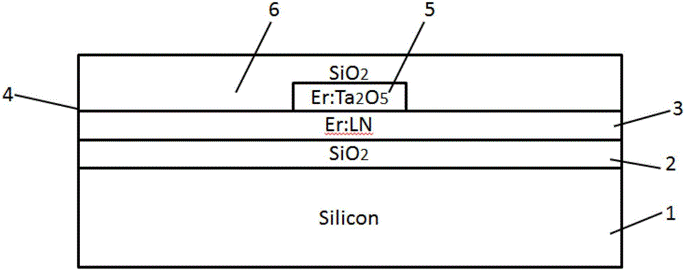
The invention discloses a manufacturing method for a waveguide amplifier with an erbium-doped tantalum oxide ridge structure. The amplifier made by the method comprises a substrate, a silica lower cladding, an erbium-doped lithium niobate film layer, a silica buffer layer, an erbium-doped tantalum oxide ridge waveguide structure, and a silica upper cladding. A silicon substrate lithium niobate film is used as a chip. The erbium-doped tantalum oxide whose refractive index is close to the refractive index of the lithium niobate is used as the ridge structure. In a communication band, through amplification effect of erbium ions, optical loss caused by processes of optical transmission and modulation can be made up. Compared with a dry etching technology, the manufactured ridge structure is low in process cost, and high in finished product rate, and stability of a device is improved. The manufacturing method is advantaged by simple manufacturing process, small device dimensions, small bending radius, and good stability.
Need to check novelty before this filing date? Find Prior Art

Description

technical field

[0001] The invention belongs to the technical field of optical communication, and in particular relates to a preparation method of a waveguide amplifier with an erbium-doped tantalum oxide ridge structure. Background technique

[0002] In the 21st century with the rapid development of science and technology, information network has become an indispensable part of people's life. The application of the network is more and more extensive, and the speed and capacity of the traditional electro-optical network can no longer meet people's needs. Optical fiber communication technology has become a new direction for the development of communication technology by virtue of its advantages of wide frequency band, low loss, immunity to electromagnetic wave interference and abundant resources.

[0003] In actual optical fiber communication, loss phenomena such as absorption, scattering and bending inevitably exist. At present, the loss coefficient of the general standard...

Examples

Embodiment Construction

[0033] The present invention will be further described below with reference to the accompanying drawings and examples, and the embodiments of the present invention include but not limited to the following examples.

[0034] Embodiment: In order to achieve the above object, the technical scheme adopted in the present invention is as follows:

[0035] Such as figure 1 As shown, the present invention provides a method for preparing a waveguide amplifier with an erbium-doped tantalum oxide ridge structure, comprising the following steps:

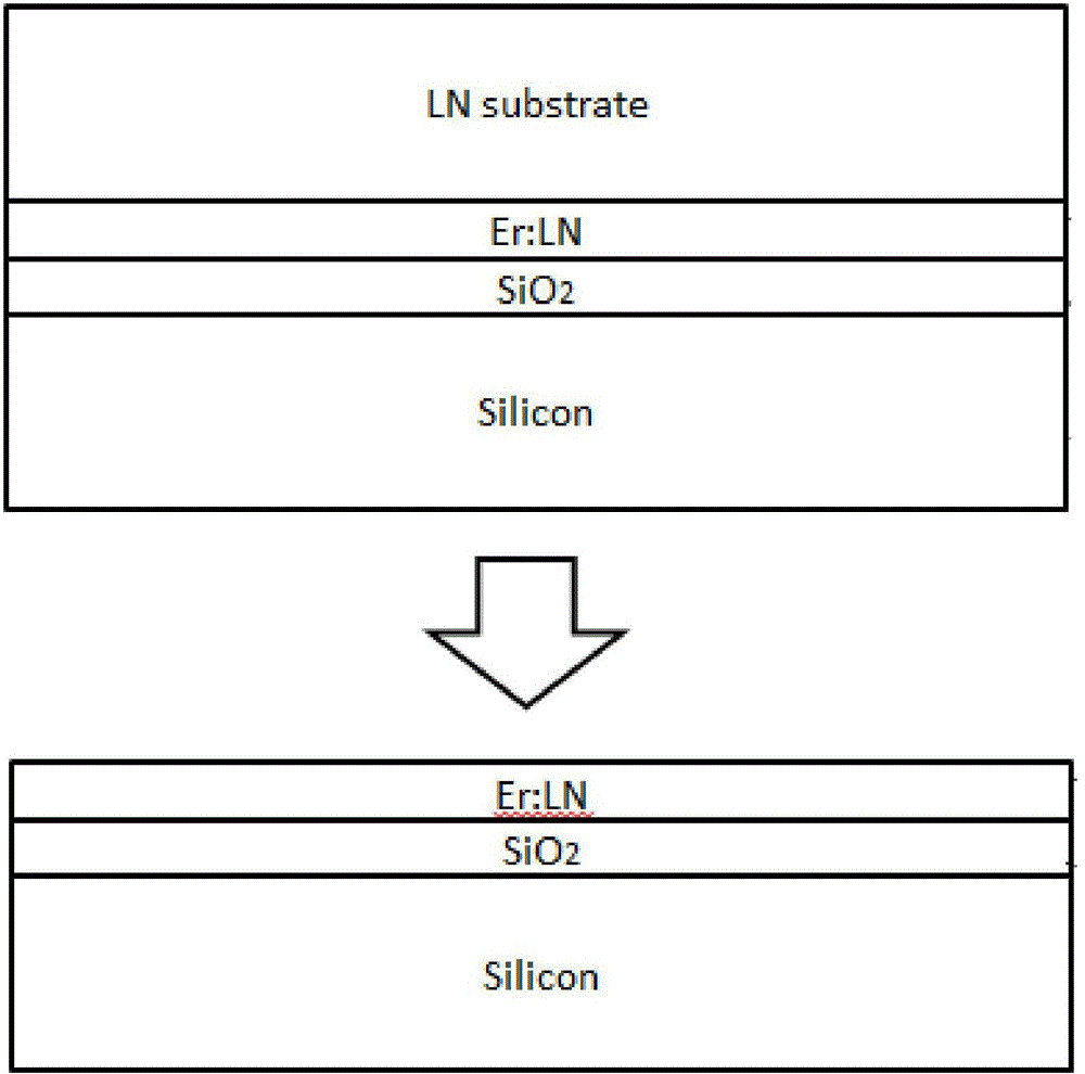
[0036] (1) Select optical-grade double-throwing 0.5mm thick lithium niobate single crystal as the initial material, clean the wafer and plate 10-20nm metal erbium on the surface, and oxidize it in the air at 1100°C to form partially erbium-doped niobium Lithium oxide crystal, the doping concentration of erbium is 0.5-1.5mol%, and a layer of local erbium-doped lithium niobate single crystal thin film is formed on the erbium-doped surface of the ...