A kind of manufacturing method of LED metal base circuit board
A technology for metal-based circuit boards and manufacturing methods, which is applied in printed circuit manufacturing, circuit substrate materials, and manufacturing printed circuit precursors, etc., can solve the problems of waste of raw materials, slow production speed, low efficiency, etc. Strong performance and good heat dissipation effect
- Summary
- Abstract
- Description
- Claims
- Application Information
AI Technical Summary
Problems solved by technology
Method used
Image
Examples
Embodiment 1
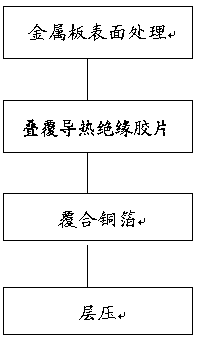
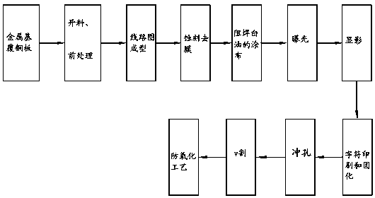
[0029] refer to figure 1 , figure 2 As shown, a method for manufacturing an LED metal-based circuit board usually includes two parts: making a metal-based copper-clad laminate and making a metal-based circuit board based on it. The steps include:
[0030] Manufacture of metal-based copper clad laminates
[0031] (1) Surface treatment of the metal plate: select an aluminum plate with a thickness of 0.2 mm, degrease, roughen, clean, and dry the surface to obtain an aluminum base plate.
[0032] (2) Overlapping thermally conductive insulating film: it is to laminate the thermally conductive insulating film on the aluminum substrate, among which there are three types of insulating adhesive, among which there are three types of insulating adhesive, ① thermally conductive PP composed of glass cloth and thermally conductive adhesive, ② with Ordinary PP composed of glass cloth and epoxy resin, ③ thermally conductive adhesive film composed of thermally conductive adhesive. And the ...
Embodiment 2
[0046] First, a 1.5mm aluminum plate is selected. The step (5) is different from that of Example 1. This example adopts a printing process to realize circuit diagram formation. The UV curing energy on the surface is 650mj to form a pattern on the substrate surface, and then the copper foil surface is printed and UV cured to form a circuit pattern on the surface of the board. Other steps are the same as in Example 1.
[0047] In the present invention, a copper plate with a thickness of 0.1 mm or 0.2 mm can be selected, and the other steps are the same as in Embodiment 2 to manufacture an integrated LED circuit board integrating a driving electric light source.
Embodiment 3
[0049] First, a 1mm aluminum plate is selected, and step (5) is different from Example 1. In this example, a printing process is used to realize circuit diagram formation. The printing process is printed with UV ink. The UV curing energy of the substrate is 800mj to form a pattern on the substrate surface, and then the copper foil surface is printed and UV cured to form a circuit pattern on the substrate surface. The other steps are the same as in Example 1.
[0050] In the present invention, metal substrates such as iron plates or silicon steel plates can also be selected as substrate materials. In step (5), the exposure process is used to realize the formation of circuit diagrams, and other steps are the same as in embodiment 3.
PUM
 Abstract
Description
Claims
Application Information

