Method of forming semiconductor device

A semiconductor and device technology, applied in the field of semiconductor device formation, can solve problems such as electrical performance to be improved, and achieve the effects of avoiding electrical parameter drift, improving electrical performance, and reducing leakage current

Active Publication Date: 2016-11-23
SEMICON MFG INT (SHANGHAI) CORP
View PDF5 Cites 3 Cited by
  • Summary
  • Abstract
  • Description
  • Claims
  • Application Information

AI Technical Summary

Problems solved by technology

[0005] However, the electrical performance of semiconductor devices

Method used


Image

  • Method of forming semiconductor device
  • Method of forming semiconductor device
  • Method of forming semiconductor device

Examples


Embodiment Construction

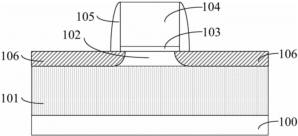
[0035] It can be seen from the background art that the electrical performance of the semiconductor device formed by using the SOI substrate in the prior art still needs to be improved.

[0036] Research on semiconductor devices found that in semiconductor devices fabricated on SOI substrates, the reference figure 1 , The material of the insulating layer 101 is usually silicon oxide, and silicon oxide has strong insulating properties. However, limited by the formation process of the insulating layer 101 , the insulating layer 101 usually has structural defects such as cracks, crystal boundaries, grain boundaries, dislocations, gaps or point defects.

[0037]When the semiconductor device is in the working state, under the influence of the voltage applied on the source, drain and gate structures, the structural defects in the insulating layer 101 will release or trap charge carriers, and the charge carriers are electrons or vacancies. holes, so that a large amount of trapped cha...


PUM

PropertyMeasurementUnit
Thicknessaaaaaaaaaa

Abstract

A method of forming a semiconductor device comprises the following steps: providing a first substrate, an insulating layer on the surface of the first substrate, and a second substrate on the surface of the insulating layer; doping the insulating layer, and forming a trap charge inhibition layer in the insulating layer, wherein the bottom surface of the trap charge inhibition layer is below the bottom surface of the insulating layer; forming a gate structure on the second substrate above the trap charge inhibition layer, wherein the trap charge inhibition layer is at least disposed right under the gate structure; forming an interlayer dielectric layer on the surface of the second substrate, wherein the interlayer dielectric layer covers the sidewall surfaces of the gate structure; and forming doped regions in the second substrate at the two sides of the gate structure. According to the invention, trap charge accumulation in the insulating layer right under the gate structure can be avoided, so that the electric field intensity in the insulating layer right under the gate structure is prevented from being too high, the leakage current of the semiconductor device is reduced, and the electrical performance of the semiconductor device is improved.

Description

technical field [0001] The invention relates to the technology in the field of semiconductor manufacturing, in particular to a method for forming a semiconductor device. Background technique [0002] With the advancement of semiconductor technology, integrated circuits are developing towards high integration, high speed and low power consumption. The process of bulk silicon (Bulk Silicon) substrates and bulk silicon devices (devices manufactured based on bulk silicon substrates) is approaching Physical limits, severe challenges are encountered in further reducing the feature size of integrated circuits. At present, the industry believes that silicon-on-insulator (SOI: Silicon on Insulator) substrates and SOI devices are one of the best solutions to replace bulk silicon and bulk silicon devices. [0003] SOI substrate is a kind of substrate used in the manufacture of integrated circuits. Compared with bulk silicon substrates currently widely used, SOI substrates have many ad...

Claims


Application Information

Patent Timeline
IPC IPC(8): H01L21/336H01L21/265
Inventor 赵猛
Owner SEMICON MFG INT (SHANGHAI) CORP
Why Eureka
Try Eureka