Semiconductor structure and formation method thereof

A semiconductor and gate structure technology, applied in the field of semiconductor structure and its formation, can solve the problems of dopant ion diffusion, source and drain surface damage, source and drain doping ion loss, etc., to achieve the effect of avoiding diffusion and reducing resistance

Active Publication Date: 2016-11-23
SEMICON MFG SOUTH CHINA CORP +1
View PDF6 Cites 19 Cited by
  • Summary
  • Abstract
  • Description
  • Claims
  • Application Information

AI Technical Summary

Problems solved by technology

[0005] In the prior art, ion doping is usually performed on the source and drain electrodes of FinFETs by source-drain ion implantation, but since ion implantation is likely to cause lattice damage, annealing is required after ion implantation to activate the dopant ions At the same time, lattice damage is repaired. During the annealing process, dopant ions are prone to diffuse, which reduces the concentration of dopant ions in the source and drain electrodes; and, after forming the source and drain electrodes, it is necessary to form a dielectric layer on the surface of the transistor, and then etch Etching the dielectric layer to form a contact hole on the surface of the source and drain, and then forming a metal silicide on the surface of the source and drain, the process of etching the dielectric layer to form a contact hole is also easy to cause damage to the surface of the source and drain, so that the source Dopant ion loss in the drain
Therefore, it is difficult to increase the concentration of dopant ions in the source and drain electrodes in the prior art, so that the performance of the fin field effect transistor formed by the prior art needs to be further reduced.

Method used


Image

  • Semiconductor structure and formation method thereof
  • Semiconductor structure and formation method thereof
  • Semiconductor structure and formation method thereof

Examples


Embodiment Construction

[0032] As mentioned in the background art, the performance of the fin field effect transistor formed in the prior art still needs to be further improved.

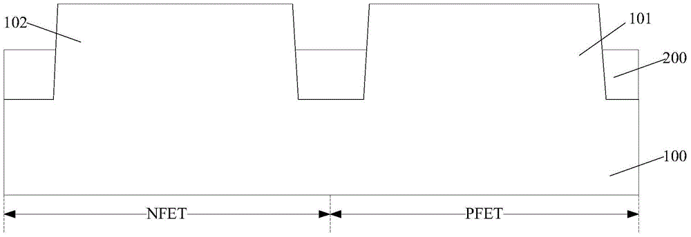
[0033]In an embodiment of the present invention, after the first gate structure spanning the first fin and the first source and drain regions located on both sides of the first gate structure are formed on the semiconductor substrate, a structure covering the first gate is formed. structure and the dielectric layer of the first source and drain region, and then etch the dielectric layer to form a first contact hole on the surface of the first source and drain region, and form an N-type doped first semiconductor epitaxy on the surface of the first source and drain region layer, and then directly form a metal silicide layer on the surface of the first semiconductor epitaxial layer, which can avoid the loss of dopant ions in the first semiconductor epitaxial layer and avoid the decrease of dopant ion concentration, thereby redu...


PUM


Abstract

The invention provides a semiconductor structure and a formation method thereof. The formation method of the semiconductor structure is that a semiconductor substrate is provided, the semiconductor substrate comprises a first region, a first fin part is formed on the first region, and an isolation layer is also formed on the semiconductor substrate; a first gate electrode structure crossing the first fin part is formed on the isolation layer; a first source-drain region is formed in the first fin part of the two sides of the first gate electrode structure; a dielectric layer is formed on the semiconductor substrate, and the dielectric layer covers the semiconductor substrate, the first fin part, the first gate electrode structure and the first source-drain region; the dielectric layer on the first region is etched so that a first contact hole arranged on the surface of the first source-drain region is formed; a first semiconductor epitaxial layer is formed on the surface of the first source-drain region, and the first type of doping ions are enabled to be doped in the first semiconductor epitaxial layer by using an in-situ doping technology; a metal silicide layer is formed on the surface of the first semiconductor epitaxial layer; and a metal plug fully filling the first contact hole is formed. According to the method, parasitic resistance of the formed semiconductor structure can be reduced.

Description

technical field [0001] The invention relates to the technical field of semiconductors, in particular to a semiconductor structure and a forming method thereof. Background technique [0002] With the continuous development of semiconductor process technology, process nodes are gradually reduced, and gate-last (gate-last) process has been widely used to obtain an ideal threshold voltage and improve device performance. However, when the feature size of the device is further reduced, even if the gate-last process is adopted, the structure of the conventional MOS field effect transistor can no longer meet the requirements for device performance, and the fin field effect transistor (Fin FET) is obtained as a multi-gate device. received widespread attention. [0003] For fin field effect transistors, as the size of the transistor continues to shrink, the parasitic resistance of the source and drain of the transistor has a more significant impact on the performance of the transisto...

Claims


Application Information

Patent Timeline
Patent Type & Authority Applications(China)
IPC IPC(8): H01L21/8238H01L27/092H01L21/336H01L29/78H01L29/08
CPCH01L21/823821H01L27/0924H01L29/0847H01L29/66795H01L29/785
Inventor 谢欣云
Owner SEMICON MFG SOUTH CHINA CORP
Why Eureka
Try Eureka