
Non-volatile memory

A non-volatile, memory technology, used in electrical solid state devices, semiconductor devices, electrical components, etc., can solve the problems of reducing the reliability of memory components, affecting the electrical performance of memory cells, and depleting the tunnel oxide layer. The effect of erasing voltage, increasing speed, and increasing coupling rate

Active Publication Date: 2016-11-23
IOTMEMORY TECH +1
View PDF10 Cites 0 Cited by
  • Summary
  • Abstract
  • Description
  • Claims
  • Application Information

AI Technical Summary

Problems solved by technology

However, the shortening of the gate length will shorten the channel length (Channel Length) under the tunnel oxide layer, which will easily cause abnormal electrical penetration (Punch Through) between the drain and the source, which will seriously affect the memory cell. electrical performance
Moreover, when programming and / or erasing memory cells, electrons repeatedly pass through the tunnel oxide layer, which will wear out the tunnel oxide layer, resulting in reduced reliability of the memory element.

Method used


Image

  • Non-volatile memory
  • Non-volatile memory
  • Non-volatile memory

Examples


Embodiment Construction

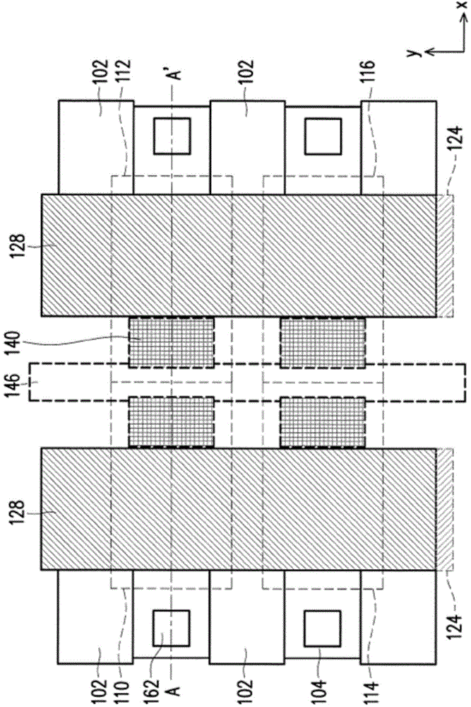
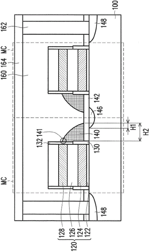
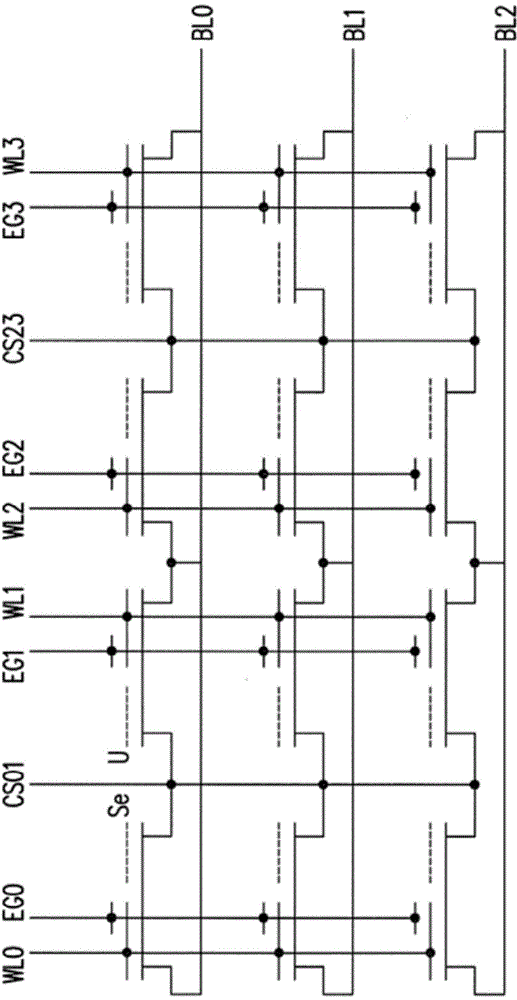
[0085] Figure 1A It is a top view of a non-volatile memory shown in the first embodiment of the present invention. Figure 1B It is a schematic cross-sectional view of a non-volatile memory shown in the first embodiment of the present invention. Figure 1B shown as along the Figure 1A Sectional view of line A-A' in the middle. Figure 1C It is a schematic circuit diagram of a non-volatile memory shown in the first embodiment of the present invention.

[0086] Please refer to Figure 1A and Figure 1B , the nonvolatile memory includes a plurality of memory cells MC. These memory cells MC are arranged in a row / column array.

[0087] The nonvolatile memory is disposed on the substrate 100 . For example, a plurality of isolation structures 102 arranged regularly are disposed in the substrate 100 to define a grid-like active region 104 . The isolation structure 102 is, for example, a shallow trench isolation structure.

[0088] Each memory cell MC includes a stack structure...


PUM


Abstract

The invention provides a nonvolatile memory, comprising a storage unit. The storage unit has a stack structure, a floating grid, a tunneling dielectric layer, an erasing grid dielectric layer, an auxiliary grid dielectric layer, a first doped zone and a second doped zone; the stack structure has the grid dielectric layer, an auxiliary grid, an insulation layer and an erasing grid which are successively arranged; the floating gate is arranged on the side wall of the first side of the stack structure; the tunneling dielectric layer is arranged under the floating grid; the erasing grid dielectric layer is arranged between the erasing grid and the floating grid; the auxiliary grid dielectric layer is arranged between the auxiliary grid and the floating grid; the first doped zone is adjacent to the floating grid; part of the first doped zone extends to the part under the floating grid; the second doped zone boards on the second side of the stack structure; and the first side is opposite to the second side. The non-volatile memory can improve an integration degree, realizes low voltage operation and improves reliability of the semiconductor.

Description

technical field [0001] The present invention relates to a semiconductor element and its manufacturing method, and in particular to a non-volatile memory. Background technique [0002] Non-volatile memory has been widely used in personal computers and electronic devices due to its advantages that data can be stored, read, and erased multiple times, and the stored data will not disappear after power failure. [0003] A typical non-volatile memory is designed to have a stacked gate (Stack-Gate) structure, which includes a tunnel oxide layer, a floating gate (Floating gate), and an inter-gate dielectric that are sequentially arranged on the substrate. layer and control gate (Control Gate). When programming or erasing the flash memory device, apply appropriate voltages to the source region, drain region, and control gate, respectively, to inject electrons into the polysilicon floating gate, or to float electrons from the polysilicon Pull out the grid. [0004] In the operation...

Claims


Application Information

Patent Timeline
Patent Type & Authority Applications(China)
IPC IPC(8): H01L27/115H01L29/423H10B41/30H10B69/00
Inventor 郑育明
Owner IOTMEMORY TECH
Features
  • Generate Ideas
  • Intellectual Property
  • Life Sciences
  • Materials
  • Tech Scout
  • Unparalleled Data Quality
  • Higher Quality Content
  • 60% Fewer Hallucinations
Learn More