

Preparation method and application of organic semiconductor two-dimensional molecular crystal material
A technology of organic semiconductors and molecular crystals, applied in the fields of semiconductor/solid-state device manufacturing, semiconductor devices, organic chemistry, etc. and other problems, to achieve the effect of easy preparation of different electronic and optoelectronic devices, saving of raw materials, and simple and easy method.
Active Publication Date: 2018-06-29
INST OF CHEM CHINESE ACAD OF SCI
View PDF4 Cites 0 Cited by
- Summary
- Abstract
- Description
- Claims
- Application Information
AI Technical Summary
Problems solved by technology
However, the two-dimensional molecular crystals prepared based on the above methods are small in size, and the method is not universal, and only works on a very small number of organic semiconductor materials, which neither meets the needs of subsequent circuit integration nor is conducive to the expansion of two-dimensional molecular crystals. The research scope of this carrier has greatly restricted the development process of the two-dimensional molecular crystal research field. To develop an experimental method for preparing two-dimensional molecular crystals with good universality, easy operation, low cost and mass production capacity, is an urgent need
Method used
View moreImage
Smart ImageViewing Examples

Examples
Embodiment 1
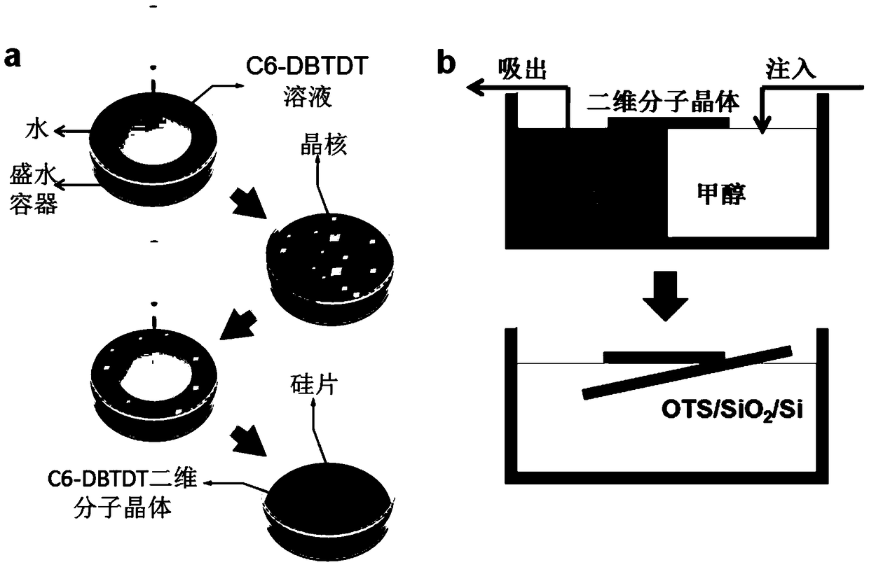
[0045] Embodiment 1, preparation C6-DBTDT two-dimensional molecular crystal structure
[0046] 1. Preparation and transfer of C6-DBTDT two-dimensional molecular crystal structure
Login to View More PUM
| Property | Measurement | Unit |
|---|---|---|
| length | aaaaa | aaaaa |
| length | aaaaa | aaaaa |
| thickness | aaaaa | aaaaa |
Abstract
The present invention provides an organic semiconductor two-dimensional molecular crystal material preparation method and application. The preparation method comprises: an organic semiconductor compound solution is dropped at the water surface, after the solution is volatilized, and an organic semiconductor two-dimensional molecule crystal nucleus is obtained at the water surface; and the organic semiconductor compound solution is continuously dropped at the organic semiconductor two-dimensional molecule crystal nucleus and is still standing, and the organic semiconductor two-dimensional molecule crystal materials are obtained on the water surface. The application of the organic semiconductor two-dimensional molecule crystal materials in the preparation field effect transistor device also belongs to the protection range of the invention. The water surface and a seed crystal formed on the water surface in advance are taken as a growth core, the solution is subjected to self assembly, a large-scale two-dimensional molecule crystal structure is grew up on the water surface, and the field effect transistor prepared by the two-dimensional molecule crystal structure has high carrier mobility and low threshold voltage.
Description
technical field [0001] The invention belongs to the technical field of organic semiconductor materials, and in particular relates to a preparation method and application of an organic semiconductor two-dimensional molecular crystal material. Background technique [0002] The so-called two-dimensional crystal means that the thickness of the crystal is only one atom thick, and the crystal is more like a huge two-dimensional molecule in essence. Two-dimensional crystals have shown great potential application value in flexible devices and wearable devices due to their extremely high flexibility and light transmission. On the one hand, compared with the corresponding three-dimensional bulk materials, two-dimensional crystals can not only show enhanced material intrinsic properties, but also may produce some new properties that bulk materials do not have due to quantum localization effects; on the other hand, ultra-thin thickness The two-dimensional crystals are considered to be ...
Claims
Login to View More Application Information
Patent Timeline
 Patent Type & AuthorityPatents(China)
IPC IPC(8): H01L51/30H01L51/40H01L51/46H01L51/48H01L51/54H01L51/56C07D495/04
CPCY02E10/549
Inventor胡文平徐春晖甄永刚董焕丽张小涛
OwnerINST OF CHEM CHINESE ACAD OF SCI