Silicon-carbide power device of heterojunction terminal and preparation method of silicon-carbide power device
A power device and heterojunction technology, which is applied in semiconductor/solid-state device manufacturing, semiconductor devices, electrical components, etc., can solve the problems of N-type SiC surface doping characteristics change, affecting low device turn-on voltage, and restricting industrialization development. , to avoid the influence of doping characteristics, high breakdown voltage, and reduce the requirements of high temperature and complex processes
- Summary
- Abstract
- Description
- Claims
- Application Information
AI Technical Summary
Problems solved by technology
Method used
Image


Examples
Embodiment 1
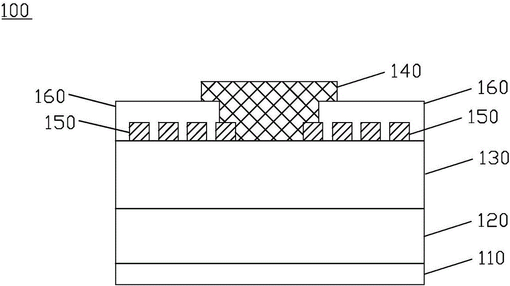
[0030] refer to figure 1 , the silicon carbide power device of this embodiment is a silicon carbide Schottky barrier diode (SBD) 100, which includes a cathode electrode 110, a substrate layer 120, an N-type SiC epitaxial layer 130, and an anode electrode 140 from bottom to top, wherein the anode electrode 140 A metal-semiconductor Schottky contact is formed with the N-type SiC epitaxial layer 130 . On the N-type SiC epitaxial layer 130 , there are several P-type structures 150 at intervals on the periphery of the anode electrode 140 to form junction terminals. In areas other than the anode electrode 140 , the exposed N-type SiC epitaxial layer 130 and the P-type structure 150 are covered with a dielectric layer 160 .
[0031] The P-type structure 150 is directly formed on the N-type SiC epitaxial layer 130 by heteroepitaxial growth of a P-type semiconductor material whose growth temperature is lower than that of SiC. Specifically, the growth temperature of the P-type semicon...
Embodiment 2
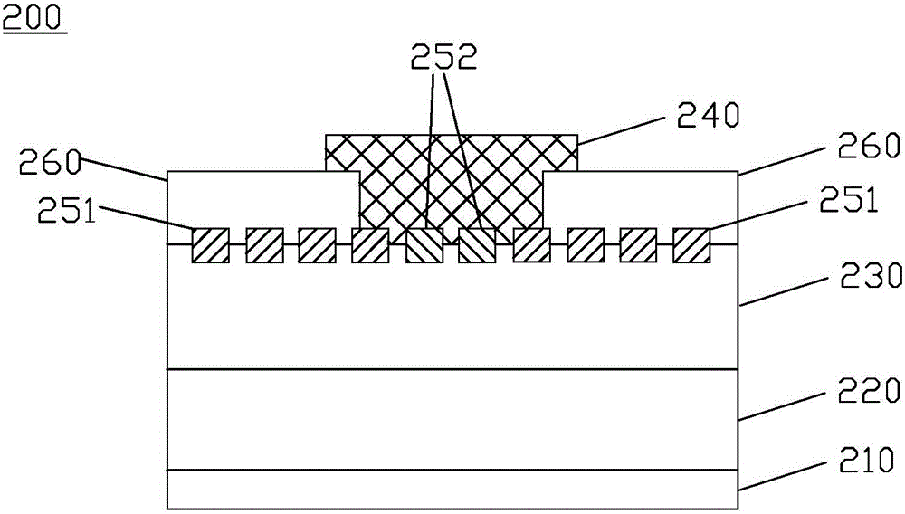
[0038] refer to figure 2 , the silicon carbide power device of this embodiment is a silicon carbide junction barrier Schottky diode 200, which differs from Embodiment 1 in that the P-type structure is distributed on the N-type SiC epitaxial layer 230 except for the P type structure 251 to form a heterojunction terminal, it also includes several discrete P-type structures 252 arranged between the anode electrode 240 and the N-type SiC epitaxial layer 230 to form a junction barrier. Specifically, the P-type structures 252 can be several parallel The strip structure forms several discretely arranged PN junctions with the N-type SiC epitaxial layer 230, and the exposed N-type SiC epitaxial layer 230 between adjacent P-type structures 252 is in contact with the anode electrode 240 to form a Schottky junction. In the reverse blocking state, the pinch-off effect of the depletion region of the adjacent PN junction is used to obtain blocking characteristics similar to that of the PN d...
Embodiment 3
[0042] refer to image 3 The silicon carbide power device of this embodiment is a silicon carbide PN junction diode 300. The difference between it and Embodiment 2 is that the P-type structure is distributed on the N-type SiC epitaxial layer 330 except for the P-type structure 351 on the periphery of the anode electrode 340. In addition to forming the heterojunction terminal, it also includes a layered P-type structure 352 disposed between the anode electrode 340 and the N-type SiC epitaxial layer 330 and isolating the anode electrode 340 and the N-type SiC epitaxial layer 330 . A PN junction is formed between the P-type structure 352 and the N-type SiC epitaxial layer 330 . For the remaining structures, such as the cathode electrode 310 , the substrate layer 320 and the dielectric layer 360 , refer to Embodiment 1, and refer to Embodiment 2 for the manufacturing method, so no further description is given.
PUM
| Property | Measurement | Unit |
|---|---|---|
| Growth temperature | aaaaa | aaaaa |
| Doping concentration | aaaaa | aaaaa |
| Doping concentration | aaaaa | aaaaa |
Abstract
Description
Claims
Application Information
 - Generate Ideas
- Intellectual Property
- Life Sciences
- Materials
- Tech Scout
- Unparalleled Data Quality
- Higher Quality Content
- 60% Fewer Hallucinations
Browse by: Latest US Patents, China's latest patents, Technical Efficacy Thesaurus, Application Domain, Technology Topic, Popular Technical Reports.
© 2025 PatSnap. All rights reserved.Legal|Privacy policy|Modern Slavery Act Transparency Statement|Sitemap|About US| Contact US: help@patsnap.com