Method for transferring graphene

A graphene and buffer layer technology, applied in the field of nanoscience and low-dimensional material preparation, can solve the problems of graphene structure damage, interface pollution, surface wrinkles, etc., and achieve the effects of reducing wrinkles, clean upper and lower surfaces, and low cost

Inactive Publication Date: 2016-12-07
SHANGHAI INST OF MICROSYSTEM & INFORMATION TECH CHINESE ACAD OF SCI
View PDF4 Cites 20 Cited by
  • Summary
  • Abstract
  • Description
  • Claims
  • Application Information

AI Technical Summary

Problems solved by technology

[0005] In view of the prior art described above, the object of the present invention is to provide a method for transferring graphene, which is used to solve problems such as structural damage, interface contamination, and surface wrinkles of graphene prepared by wet transfer in the prior art

Method used


Image

  • Method for transferring graphene
  • Method for transferring graphene
  • Method for transferring graphene

Examples


Embodiment 1

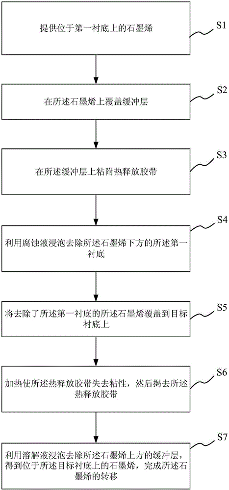
[0083] In this embodiment, a buffer layer is used to transfer the single crystal graphene grown by chemical vapor deposition (CVD) onto the target substrate.

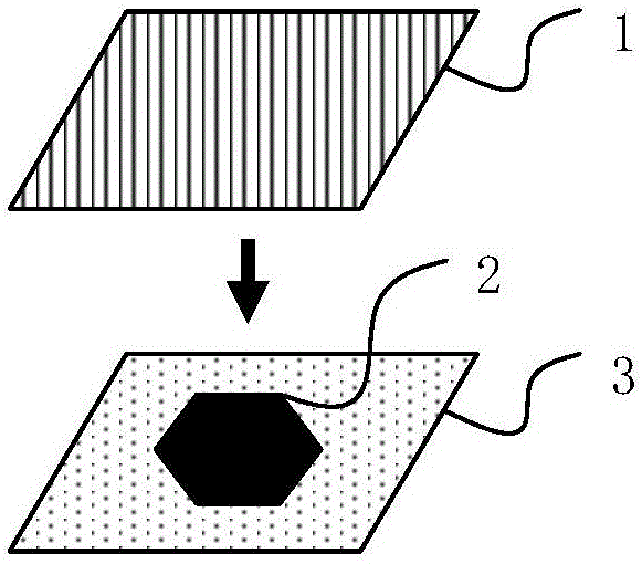
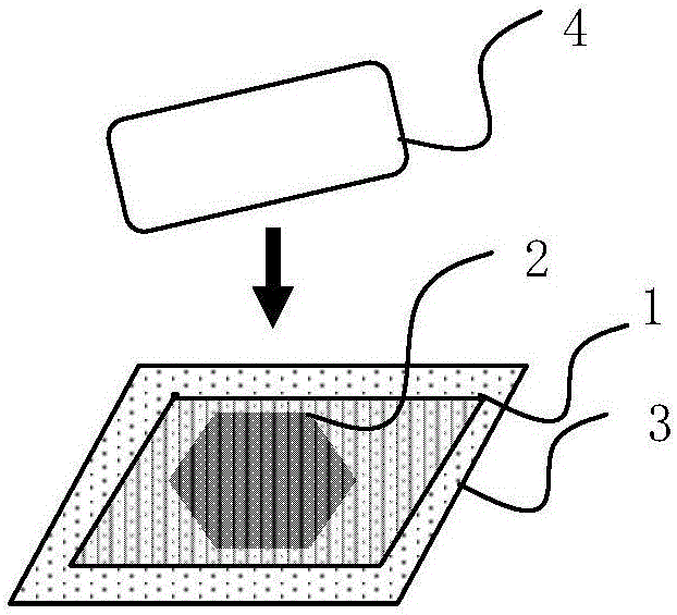
[0084] See first Figure 2 ~ Figure 3 Steps S1 and S2 are executed, and the surface of the graphene 2 on the first substrate 3 is evenly covered with the buffer layer 1 .

[0085] Specifically, graphene 2 is prepared on the first substrate 3 first. As an example, the first substrate 3 is copper foil with a thickness of 25 μm. In other embodiments, the first substrate 3 can also be selected from other catalytic substrates, such as Cu, Ni, Pt, Mo, Pd, Ge, Fe, Co or alloy substrates composed of two or three thereof Wait.

[0086] During the growth process of graphene grown by chemical vapor deposition, the growth temperature is 1000°C~1050°C, the pressure in the chamber is 20Pa~102kPa, the reducing gas is hydrogen, the inert gas is argon, and the flow rate of hydrogen is 5sccm~200sccm, argon The flow rate of the gas is...

Embodiment 2

[0101] This embodiment adopts basically the same technical solution as that of Embodiment 1, except that in Embodiment 1, a buffer layer is used to transfer the discontinuous graphene single crystal grown by CVD to the target substrate. However, in this embodiment, the continuous graphene grown by CVD method is assisted to transfer to the target substrate by using the buffer layer to obtain the continuous graphene film.

[0102] Figure 12 Shown is an optical microscope image of continuous graphene grown by chemical vapor deposition using a buffer layer in this example. Figure 13 Shown is a Raman surface scanning image of continuous graphene grown by chemical vapor deposition using a buffer layer in this example.

Embodiment 3

[0104] The difference between this example and Example 1 is that the buffer layer in Example 1 is changed to methyl methacrylate (MMA), the heating temperature is increased to 70°C, and the heating time is extended to 15 minutes. All the other process parameters are the same as in Example 1.

[0105] Compared with Example 1, as the heat resistance of the buffer layer increases, the heating temperature in the process of curing the buffer layer also increases accordingly. Appropriately increasing the curing temperature of the buffer layer will not have a great impact on the properties of graphene. Figure 14 It shows an optical microscope image of single crystal graphene obtained by changing the buffer layer of this embodiment to methyl methacrylate (MMA) assisted transfer.


PUM

PropertyMeasurementUnit
thicknessaaaaaaaaaa
thicknessaaaaaaaaaa

Abstract

The invention provides a method for transferring graphene. The method comprises the following steps: providing graphene on a first substrate; covering a buffer layer on the graphene; adhering a heat release adhesive tape on the buffer layer; soaking the first substrate in a corrosive solution to remove the first substrate under the graphene; covering the graphene without the first substrate on a target substrate; heating to make the heat release adhesive belt become non-sticky, removing the heat release adhesive belt; and soaking the buffer layer in a dissolving solution to remove the buffer layer on the graphene to obtain graphene on a target substrate to finish the transferring of graphene. According to the method, a buffer layer is used to assist the transferring of graphene, the required steps are few, the process is fast and convenient, the upper and lower surfaces of graphene are clean, no substance is adhered on the upper and lower surfaces of the graphene, the wrinkles in the microscopic level are reduced, thus the effective usable area of graphene is enlarged, and the graphene can be more suitable for being used to prepare electronic devices.

Description

technical field [0001] The invention relates to the technical fields of nanoscience and low-dimensional material preparation, in particular to a method for transferring graphene. Background technique [0002] Graphene is a single-layer two-dimensional nanomaterial with a two-dimensional honeycomb lattice structure. It has many unique physical and chemical properties. It has broad application prospects in electronic devices such as energy storage, transistors, supercapacitors, and sensors. Graphene has high strength, high specific surface area and good thermal conductivity; the quantum Hall effect at room temperature, the size effect of surface properties; each carbon atom in ideal graphene presents sp 2 The hybrid bond structure, while the excess electrons form large π bonds on the two-dimensional scale, the free movement of π electrons in the two-dimensional plane makes graphene have excellent conductivity, and its carrier mobility is as high as 20,000 cm 2 V -1 S -1 , 1...

Claims


Application Information

Patent Timeline
Patent Type & Authority Applications(China)
IPC IPC(8): C01B31/04
CPCC01B2204/04C01P2002/82C01P2004/02C01P2004/04
Inventor 陈吉吴天如王浩敏谢晓明
Owner SHANGHAI INST OF MICROSYSTEM & INFORMATION TECH CHINESE ACAD OF SCI
Why Eureka
Try Eureka