Supercharge Your Innovation With Domain-Expert AI Agents!

Preparation method for forming metal silicide on gate of semiconductor device

A metal silicide and semiconductor technology, applied in semiconductor devices, electrical components, circuits, etc., can solve the problems of damaging semiconductor devices, reducing the reliability of semiconductor devices, and leakage of semiconductor devices

Active Publication Date: 2019-01-08
FOUNDER MICROELECTRONICS INT
View PDF4 Cites 0 Cited by
  • Summary
  • Abstract
  • Description
  • Claims
  • Application Information

AI Technical Summary

Problems solved by technology

[0005] The invention provides a preparation method for forming a metal silicide on the gate of a semiconductor device, which is used to solve the problem of semiconductor device leakage caused by the existing preparation method, thereby damaging the semiconductor device and reducing the reliability of the semiconductor device

Method used


Image

  • Preparation method for forming metal silicide on gate of semiconductor device
  • Preparation method for forming metal silicide on gate of semiconductor device
  • Preparation method for forming metal silicide on gate of semiconductor device

Examples


Embodiment Construction

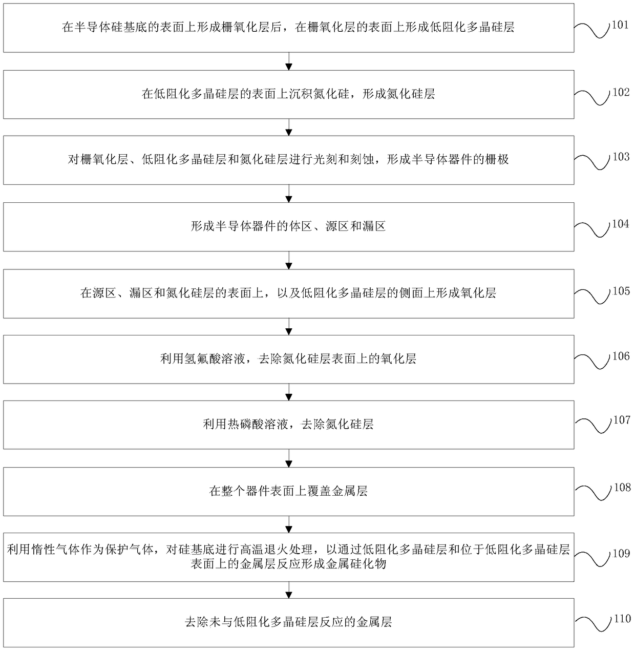
[0030] In order to make the purpose, technical solutions and advantages of the embodiments of the present invention clearer, the technical solutions in the embodiments of the present invention will be clearly and completely described below in conjunction with the drawings in the embodiments of the present invention. Obviously, the described embodiments It is a part of embodiments of the present invention, but not all embodiments. Based on the embodiments of the present invention, all other embodiments obtained by persons of ordinary skill in the art without making creative efforts belong to the protection scope of the present invention.

[0031] figure 1 It is a schematic flow chart of the method for forming a metal silicide on the gate of a semiconductor device provided in Embodiment 1 of the present invention. In order to describe the method in this embodiment clearly and systematically, as figure 1 As shown, the methods include:

[0032] Step 101, after forming a gate oxi...


PUM

PropertyMeasurementUnit
thicknessaaaaaaaaaa
thicknessaaaaaaaaaa
thicknessaaaaaaaaaa

Abstract

The invention provides a preparation method for forming a metal silicide on the gate of a semiconductor device. The method comprises: sequentially forming a gate oxide layer and a low-resistance polysilicon layer on the surface of a semiconductor silicon substrate; Deposit silicon nitride on the surface to form a silicon nitride layer; form a gate after photolithography and etching, and then form a body region, source region and drain region; form an oxide layer on the surface of the entire device; remove the surface of the silicon nitride layer The oxide layer is removed to remove the silicon nitride layer; after the metal layer is covered on the entire device surface, the metal layer on the surface of the low-resistance polysilicon layer reacts to form a metal silicide, and then the unreacted metal layer is removed. The problem of preventing the electric leakage of the semiconductor device is realized, and the reliability of the semiconductor device is improved.

Description

technical field [0001] The invention relates to the field of semiconductor technology, in particular to a preparation method for forming a metal silicide on a gate of a semiconductor device. Background technique [0002] Semiconductor devices are commonly used devices in industrial manufacturing, and metal silicide needs to be formed on the gate of the semiconductor device to reduce the resistance of the gate. [0003] The preparation method for forming a metal silicide on the gate of a semiconductor device provided in the prior art is: depositing silicon nitride on a polysilicon layer on a semiconductor silicon substrate to form a silicon nitride layer; Implant N-type ions into the polysilicon layer in the direction to make the polysilicon layer a low-resistance polysilicon layer; then perform photolithography, etching, and thermal oxidation treatments on the silicon substrate to form an oxide layer on the surface of the silicon substrate; then use acidic The solution remo...

Claims


Application Information

Patent Timeline
Patent Type & Authority Patents(China)
IPC IPC(8): H01L21/28
CPCH01L29/4933
Inventor 闻正锋马万里赵文魁
Owner FOUNDER MICROELECTRONICS INT
Features
  • R&D
  • Intellectual Property
  • Life Sciences
  • Materials
  • Tech Scout
  • Unparalleled Data Quality
  • Higher Quality Content
  • 60% Fewer Hallucinations
Learn More