
High-voltage metal oxide semiconductor field effect transistor (MOSFET) with derangement super junction P regions and manufacturing method of MOSFET

A dislocation arrangement and high-voltage technology, which is applied in semiconductor/solid-state device manufacturing, electrical components, circuits, etc., can solve the problems of device withstand voltage drop, breakdown voltage drop, etc., and achieve reduced etching trench depth and anti-charge offset The effect of enhancing the ability to influence and reducing the degree of dependence

Active Publication Date: 2016-12-07
XIAMEN YUANSHUN MICROELECTRONICS TECH +2
View PDF5 Cites 2 Cited by
  • Summary
  • Abstract
  • Description
  • Claims
  • Application Information

AI Technical Summary

Problems solved by technology

If the charge is unbalanced, the withstand voltage of the device will be seriously affected and will drop sharply. When the charge amount between the columns deviates by ±10%, the breakdown voltage of the device will drop by nearly 22%.

Method used


Image

  • High-voltage metal oxide semiconductor field effect transistor (MOSFET) with derangement super junction P regions and manufacturing method of MOSFET
  • High-voltage metal oxide semiconductor field effect transistor (MOSFET) with derangement super junction P regions and manufacturing method of MOSFET
  • High-voltage metal oxide semiconductor field effect transistor (MOSFET) with derangement super junction P regions and manufacturing method of MOSFET

Examples


Embodiment Construction

[0030] The technical scheme of the present invention will be further described below in conjunction with the accompanying drawings of the description:

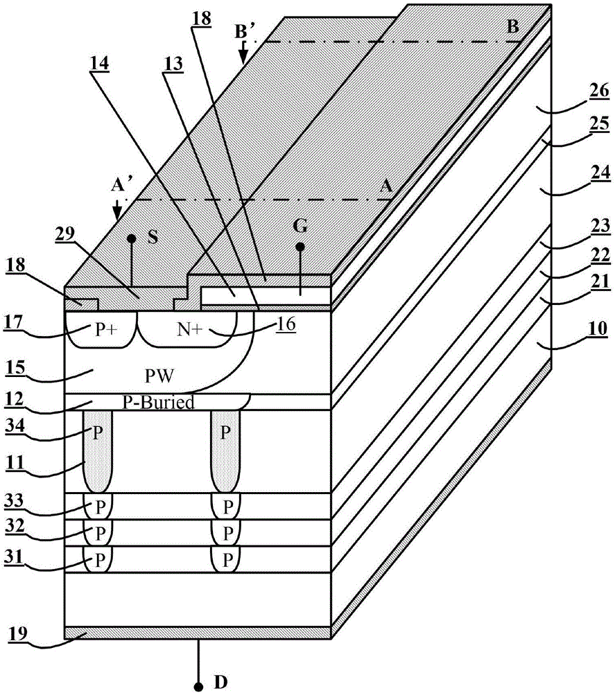
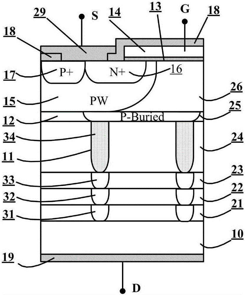
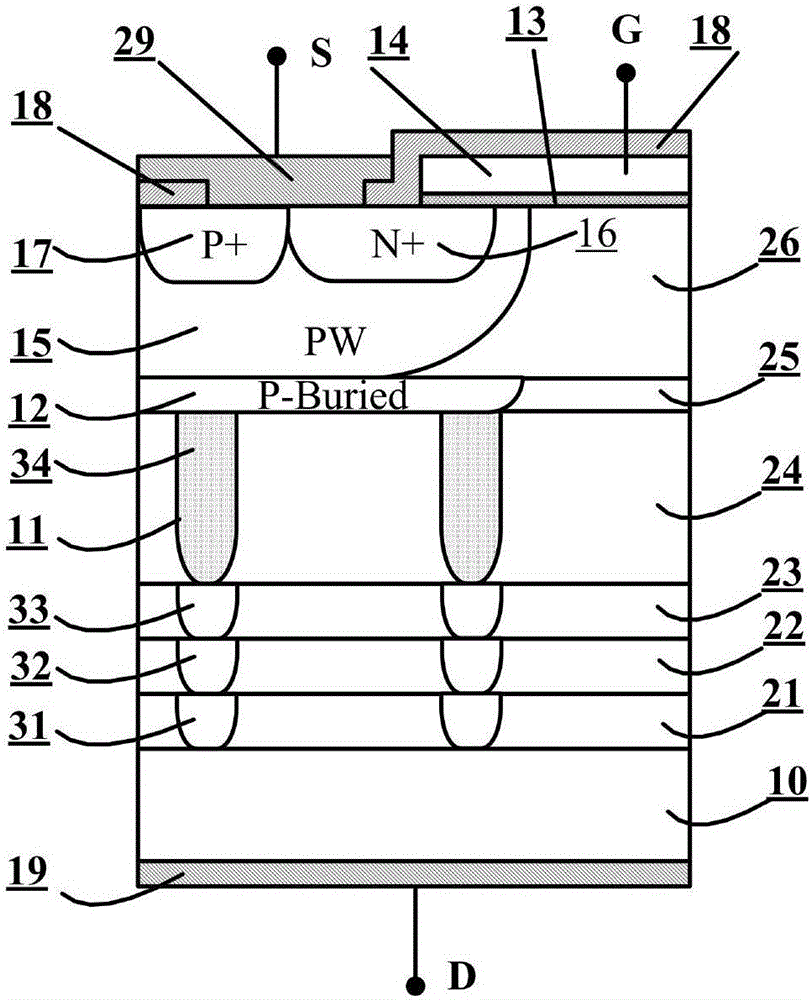
[0031] Such as Figure 1 to Figure 3 As shown, a high-voltage MOSFET with a superjunction P region arranged in dislocation, including a metal layer A19, an N+ substrate 10, a P string region, a P column region, a fifth epitaxial layer 25, a sixth epitaxial layer 26, and a gate The oxide layer 13, the metal layer B29, the polysilicon gate 14, the metal layer A19, the N+ substrate 10, the P string region, the P column region, the fifth epitaxial layer 25, and the sixth epitaxial layer 26 are arranged in sequence from bottom to top, Both the metal layer A19 and the P string region are connected to the N+ substrate 10, the P string region and the fifth epitaxial layer 25 are connected to the P column region, and the sixth epitaxial layer 26 is connected to the fifth epitaxial layer 25, the metal layer B29 and the gate oxide layer...


PUM


Abstract

The invention discloses a high-voltage MOSFET with derangement super junction P regions and a manufacturing method of the MOSFET. The MOSFET comprises a metal layer A, an N+ substrate, a P string region, a P column region, a fifth layer epitaxial layer, a sixth layer epitaxial layer, a gate oxide layer, a metal layer B and a polysilicon gate, wherein the metal layer A, the N+ substrate, the P string region, the P column region, the fifth layer epitaxial layer and the sixth layer epitaxial layer are arranged from bottom to top sequentially, the polysilicon gate is located in the gate oxide layer, the metal layer B leads out an S pole, the polysilicon gate leads out a G pole, the metal layer A leads out a D pole, and a P buried layer is arranged in the fifth layer epitaxial layer and comprises a plurality of ion implanted regions which are arranged in derangement. According to the high-voltage MOSFET, the voltage resistance value is high, the charge deviation resistance is enhanced, the reliability is improved, the technology is simple, the efficiency and the power device yield are improved, and the cost is reduced.

Description

technical field [0001] The invention relates to a high-voltage MOSFET with dislocation-arranged superjunction P regions and a manufacturing method thereof. Background technique [0002] There are two main technical routes in the manufacturing process of the existing super junction power MOSFET: 1. Deep trench etching and filling with single crystal silicon; 2. Multiple ion implantation, annealing and epitaxy. Generally, taking the 600V SJ-VDMOS as an example, the former needs to be etched to form a trench whose depth reaches or exceeds two-thirds of the thickness of the epitaxial layer, and the trench aspect ratio is higher than 20:1. The etching equipment and process put forward very high requirements; using multiple ion implantation, annealing and epitaxy technology does not require trench etching, but the complete manufacturing process must go through multiple cycles of ion implantation, annealing, epitaxy and other processes, and the process is complex , the efficiency ...

Claims


Application Information

Patent Timeline
Patent Type & Authority Applications(China)
IPC IPC(8): H01L29/78H01L29/06H01L21/336
CPCH01L29/0615H01L29/0684H01L29/66477H01L29/78
Inventor 高秀秀焦世龙高耿辉陈利
Owner XIAMEN YUANSHUN MICROELECTRONICS TECH
Learn More