


Quick Research
Generate reliable direction feasibility study reports for your R&D in just a few steps.

Technical Q&A
Discover and master advanced knowledge NOW. Basics, ideas, possibilities, all at once.

Find Solutions
As an expert in R&D theories, this can generate solutions to your technical problems instantly.

Evaluate Feasibility
Analyze your overall solution with one click, know your potential R&D risks in advance.

Monitor Landscape
Get weekly tech updates, stay abreast of the latest tech innovations and key insights.
III-nitride semiconductor light emitting device graphical substrate and preparation method
A technology of nitride semiconductors and patterned substrates, which is applied to semiconductor devices, electrical components, circuits, etc., can solve the problems of increasing the density of convex patterns A, such as the limit, and achieve the effect of increasing density
- Summary
- Abstract
- Description
- Claims
- Application Information
AI Technical Summary
Problems solved by technology
Method used
Image

Examples
Embodiment 1
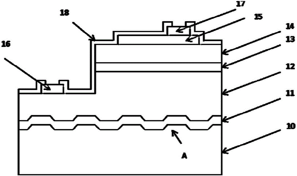
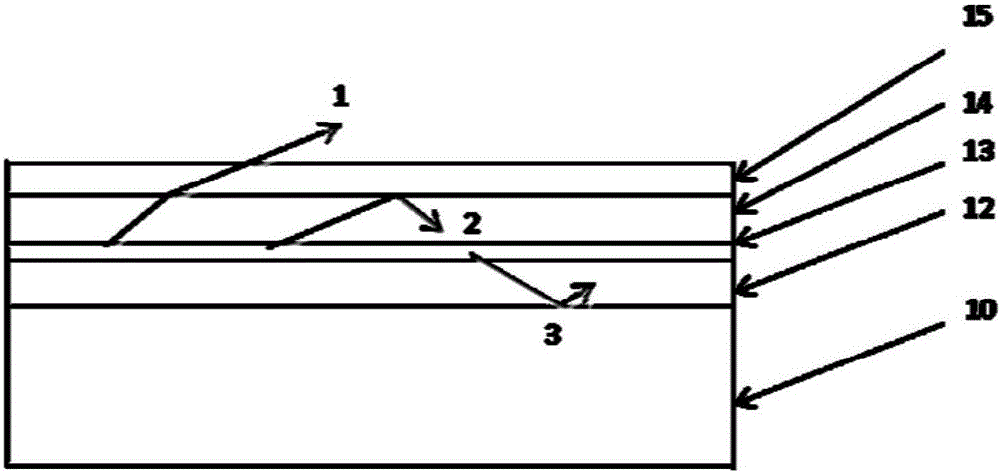
[0032] Such as Figure 4 As shown, the III-nitride semiconductor light-emitting device of the present invention includes a substrate 10, a buffer layer 11, an N-type III-nitride thin film layer 12, a light-emitting layer 13 composed of III-nitride quantum wells, and a P-type III-nitride thin film Layer 14, transparent electrode layer 15, N-type metal electrode layer 16, welding electrode 17, and light-transmitting protective film 18. The difference from traditional III-nitride semiconductor light-emitting devices is that the surface of the substrate 10 forms a stepped side wall B , the area of the inclined surface H of the stepped side wall B is maximized, the scattering efficiency of the substrate 10 is improved, and thus the external quantum efficiency is also increased.
[0033] The p-type III-nitride thin film layer 14 and the transparent electrode layer 15 are interposed by an n+ type or p+ type III-nitride semiconductor layer, or an n-type or p-type III-nitride semicon...
Embodiment 2
[0046] Figures 10a-10c It is a schematic diagram of another example of the present invention. In this example, the dry etching mask. is realized twice, and the ladder pattern B is obtained by one dry etching.
[0047] Using photolithographic plates such as Figure 10a As shown in the figure, a large-scale photolithography pattern mask 61 is formed, and then above it as Figure 10b As shown, a small-scale photolithographic pattern mask 62 is formed. The process of forming the small-scale photolithographic pattern mask 62 on the large-scale photolithographic pattern mask 61 is the same as the process of forming the large-scale photolithographic pattern mask 61 except for the size of the photoresist plate used.
Embodiment 3
[0049] Figure 11 It is a schematic diagram of another example of the present invention. and Figure 10a , 10b is different in that the same photolithography plate is used to form the first photolithography pattern mask 63 and the second photolithography pattern mask 64, and they are interlaced with each other. At this time, in the process of partially superimposing the first photolithography pattern mask 63 pattern and the second photolithography pattern mask 64 pattern, except that the position of the photoresist plate is adjusted to the position where the pattern is superimposed during exposure, other processes are the same as those in the photolithography pattern mask.
[0050] The process of forming the first photolithography pattern mask 63 on the substrate (10) is the same.
[0051] Embodiment 2 and Embodiment 3 are different from Embodiment 1 in that a dry etching process is performed to form pattern B. The specific etching method is further described as follows:
...
PUM
 Abstract
Description
Claims
Application Information
 - R&D Engineer
- R&D Manager
- IP Professional
- Industry Leading Data Capabilities
- Powerful AI technology
- Patent DNA Extraction
Browse by: Latest US Patents, China's latest patents, Technical Efficacy Thesaurus, Application Domain, Technology Topic, Popular Technical Reports.
© 2024 PatSnap. All rights reserved.Legal|Privacy policy|Modern Slavery Act Transparency Statement|Sitemap|About US| Contact US: help@patsnap.com