A kind of er-se-sb nano phase change film material and its preparation method and application

A technology of er-se-sb and thin-film materials, applied in nanotechnology, nanotechnology, nanotechnology for materials and surface science, etc., can solve problems such as poor thermal stability, low crystallization temperature, and unsatisfactory data retention , to achieve the effects of reduced power consumption, high crystallization temperature and data retention, high crystalline and amorphous resistance

Active Publication Date: 2019-01-22
JIANGSU UNIV OF TECH
View PDF3 Cites 0 Cited by
  • Summary
  • Abstract
  • Description
  • Claims
  • Application Information

AI Technical Summary

Problems solved by technology

However, a faster crystallization rate usually means a lower crystallization temperature, which often results in less than ideal data retention
[0006] Antimony-rich (Sb) nano-alloy films (phase-change alloy films in which Sb is dominant in the structure, such as Ga-Sb, Ge-Sb, Sn-Sb, etc.) have extremely high phase change speeds due to the presence of Sb (generally less than 10ns), has attracted extensive attention from researchers, but this kind of material also has the disadvantage of poor thermal stability, so improving the phase transition properties of antimony-rich nano-alloy films will become a hot topic in future research

Method used


Image

  • A kind of er-se-sb nano phase change film material and its preparation method and application
  • A kind of er-se-sb nano phase change film material and its preparation method and application
  • A kind of er-se-sb nano phase change film material and its preparation method and application

Examples


Embodiment 1

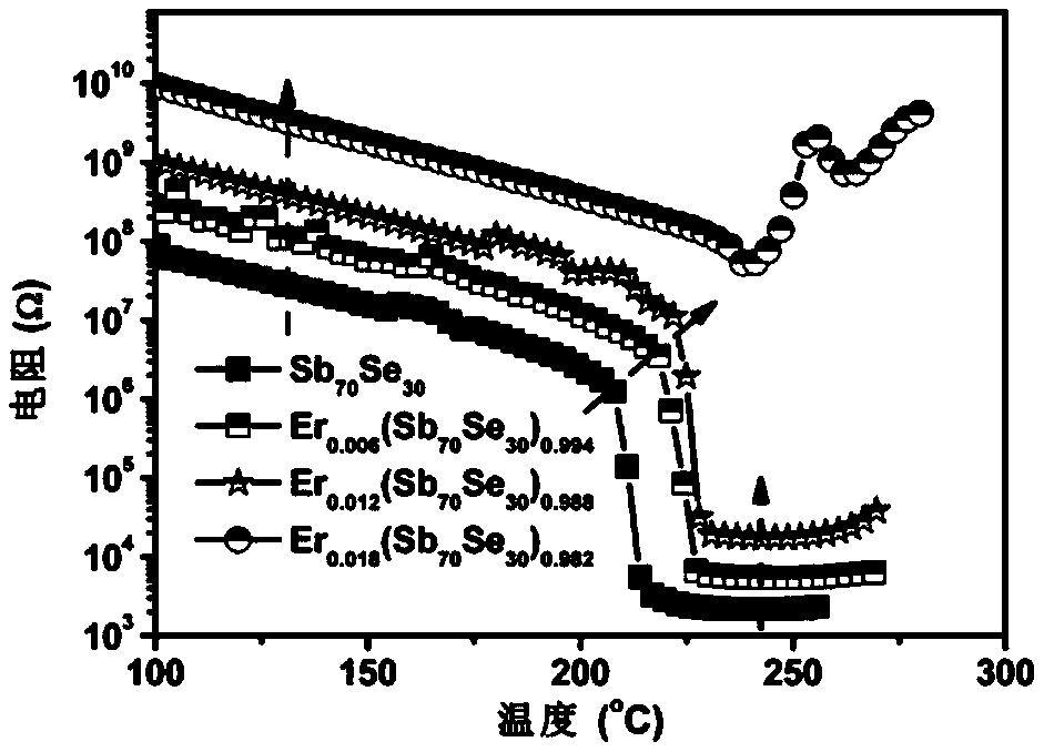
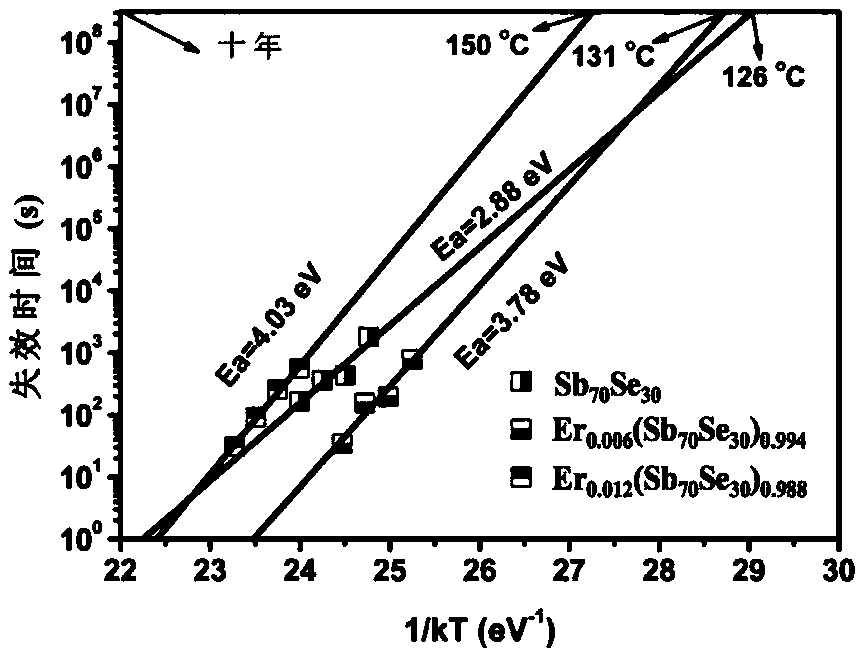
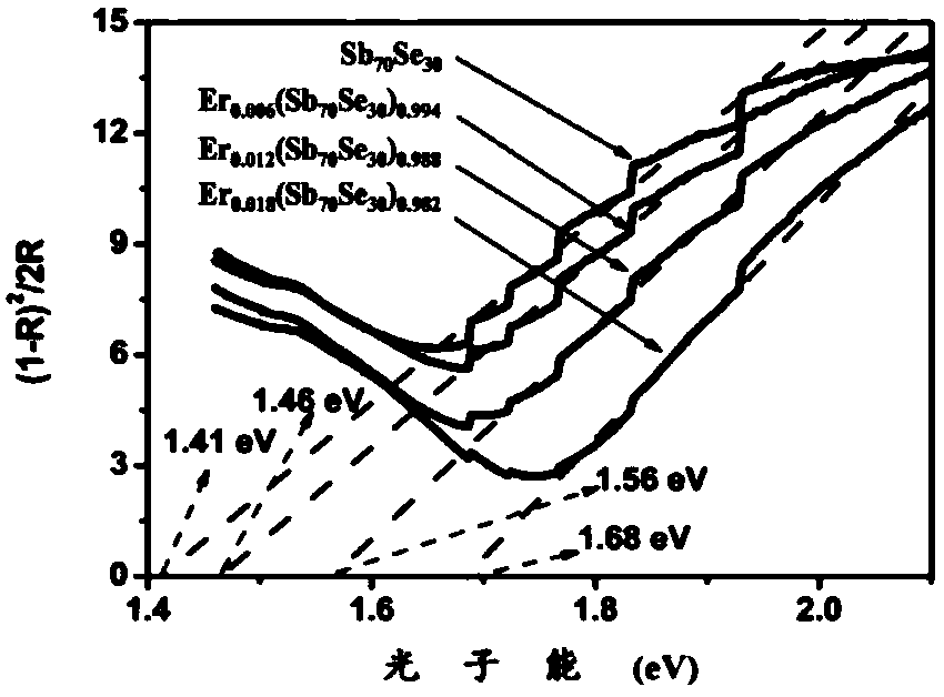
[0035] Embodiment 1: Preparation of Se without Er doping 30 Sb 70 Nano phase change thin film material.

[0036] 1. Clean SiO2 2 / Si(100) substrate surface and back, remove dust particles, organic and inorganic impurities;

[0037] a) Strong ultrasonic cleaning in acetone solution for 3 to 5 minutes, then rinse with deionized water;

[0038] b) Strong ultrasonic cleaning in ethanol solution for 3-5 minutes, rinse with deionized water, high-purity N 2 Blow dry the surface and back;

[0039] c) Dry the water vapor in an oven at 120°C for about 20 minutes.

[0040] 2. Preparation of Se by radio frequency sputtering method 30 Sb 70 Film preparation:

[0041] a) Install Se 30 Sb 70 Sputtering target (atomic percentage purity reaches 99.999%), and the background vacuum is evacuated to 1×10 -4 Pa;

[0042] b) Set the sputtering power to 30W;

[0043]c) Using high-purity argon (volume percent purity up to 99.999%) as the sputtering gas, setting the argon flow rate to 30 s...

Embodiment 2

[0048] Embodiment 2: preparation Er 0.006 (Se 30 Sb 70 ) 0.994 Nano phase change thin film material.

[0049] 1. Clean SiO2 2 / Si(100) substrate surface and back, remove dust particles, organic and inorganic impurities;

[0050] a) Strong ultrasonic cleaning in acetone solution for 3 to 5 minutes, then rinse with deionized water;

[0051] b) Strong ultrasonic cleaning in ethanol solution for 3-5 minutes, rinse with deionized water, high-purity N 2 Blow dry the surface and back;

[0052] c) Dry the water vapor in an oven at 120°C for about 20 minutes.

[0053] 2. Preparation of Er by RF sputtering method 0.006 (Se 30 Sb 70 ) 0.994 Film preparation:

[0054] a) Install Se 30 Sb 70 For the sputtering target, place a fan-shaped Er sheet with a thickness of 2mm, a diameter of 40mm, and an arc of 15° on Se 30 Sb 70 The surface of the target, so that the centers of the two circles coincide, and the background vacuum is evacuated to 1×10 -4 Pa, where Se 30 Sb 70 The...

Embodiment 3

[0061] Embodiment 3: preparation Er 0.012 (Se 30 Sb 70 ) 0.988 Nano phase change thin film material.

[0062] 1. Clean SiO2 2 / Si(100) substrate surface and back, remove dust particles, organic and inorganic impurities;

[0063] a) Strong ultrasonic cleaning in acetone solution for 3 to 5 minutes, then rinse with deionized water;

[0064] b) Strong ultrasonic cleaning in ethanol solution for 3-5 minutes, rinse with deionized water, high-purity N 2 Blow dry the surface and back;

[0065] c) Dry the water vapor in an oven at 120°C for about 20 minutes.

[0066] 2. Preparation of Er by RF sputtering method 0.012 (Se 30 Sb 70 ) 0.988 Film preparation:

[0067] a) Install Se 30 Sb 70 For the sputtering target, put two fan-shaped Er sheets with a thickness of 2mm, a diameter of 40mm, and an arc of 15° on Se 30 Sb 70 The surface of the target, so that the centers of the two circles coincide, and the background vacuum is evacuated to 1×10 -4 Pa, where Se 30 Sb 70 Th...


PUM

PropertyMeasurementUnit
thicknessaaaaaaaaaa

Abstract

The invention belongs to the technical field of nanomaterials, and relates to an Er-Se-Sb nano-phase change thin film material and a preparation method and application thereof. The thin film material of the present invention is composed of three elements, erbium, selenium and antimony, and its general chemical formula is Erx(SeySb100-y)1-x, wherein 0

Description

technical field [0001] The invention belongs to the technical field of nanometer materials, and in particular relates to an Er-Se-Sb nanometer phase-change film material and a preparation method and application thereof. Background technique [0002] In the era of globalization in the 21st century, information plays an increasing role in daily life and work. At the same time, as people communicate more and more frequently, the amount of data obtained by human society is increasing rapidly year by year. In order not to restrict the development of human civilization and realize the efficient use of information, it is necessary to realize the long-term stable storage of a large amount of information (storage is the recording and preservation of information). [0003] At present, the main products in the semiconductor memory market are dynamic memory (DRAM), static memory (SRAM) and flash memory (FLASH). Among them, flash memory occupies more than 90% of the non-volatile memory...

Claims


Application Information

Patent Timeline
Patent Type & Authority Patents(China)
IPC IPC(8): H01L45/00B82Y30/00B82Y40/00
CPCB82Y30/00B82Y40/00H10N70/881H10N70/8825H10N70/023H10N70/021H10N70/026
Inventor 邹华胡益丰朱小芹薛建忠张建豪郑龙吴世臣袁丽孙月梅吴卫华眭永兴
Owner JIANGSU UNIV OF TECH
Why Eureka
Try Eureka