Semiconductor detector

A detector and semiconductor technology, applied in semiconductor devices, instruments, measuring devices, etc., can solve problems such as increased detector noise, inconvenient installation, and potential safety hazards, and achieve improved energy resolution, reduced dark current influence, and high The effect of energy resolution

Active Publication Date: 2016-12-21
NUCTECH CO LTD
View PDF9 Cites 1 Cited by
  • Summary
  • Abstract
  • Description
  • Claims
  • Application Information

AI Technical Summary

Problems solved by technology

However, in practical applications, the high voltage of the field-enhancing electrode is directly connected to the side of the detector, usually by direct welding of high-voltage wires. The source also carries noise, which increases the noise of the detector. At the same time, a dark c

Method used


Image

  • Semiconductor detector
  • Semiconductor detector
  • Semiconductor detector

Examples


Embodiment Construction

[0023] Reference will now be made in detail to embodiments of the invention, examples of which are illustrated in the accompanying drawings, wherein like numerals refer to like elements throughout. The following embodiments will be described by referring to the figures in order to explain the present invention.

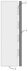
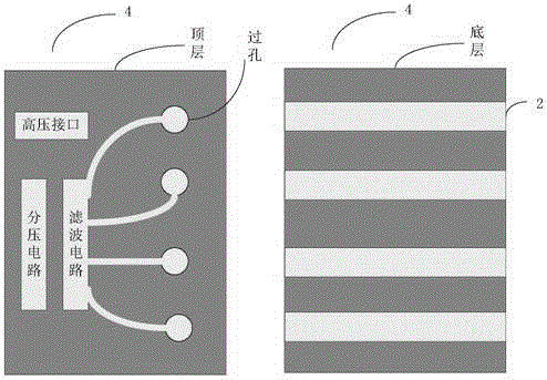
[0024] The present invention adds an insulating substance on the surface of the field-enhancing electrodes and the detector, which can reduce the impact of side field-enhancing high voltage noise on the detector, and also reduce the dark current between the field-enhancing electrodes, thereby improving the energy resolution of the detector.

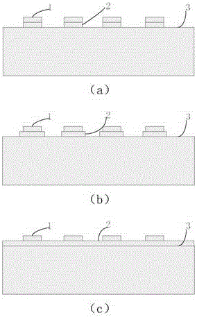
[0025] figure 1 A side view showing the structure of a semiconductor detector according to an embodiment of the present invention. Such as figure 1 As shown, the semiconductor detector includes a semiconductor detector material 3, which can be CZT (Cadmium zinc telluride), CdTe (cadmium telluride), CdMnTe (cadmium manganese tel...


PUM


Abstract

The invention brings forward a semiconductor detector. The semiconductor detector comprises a detector crystal which comprises a crystal main body, an anode and a cathode; field enhancement electrodes used for applying voltages to the detector crystal; and insulation materials arranged between the field enhancement electrodes and the surface of the detector crystal. The semiconductor detector further comprises a field enhancement electrode circuit board, the field enhancement electrode circuit board is provided with a bottom connection layer in contact with the surface of the detector crystal and a top surface opposite to the bottom connection layer, the top layer is connected with high-voltage input of the semiconductor detector, and the insulation materials exist between the bottom connection layer and the detector surface of the detector crystal.

Description

technical field [0001] The invention relates to a semiconductor detector, in particular to a semiconductor detector, and more specifically to a field-enhanced line electrode CdZnTe semiconductor detector. Background technique [0002] Due to its relatively uniform electric field distribution, the field-enhanced semiconductor detector greatly improves the energy resolution and peak-to-valley ratio of the detector. However, in practical applications, the high voltage of the field-enhancing electrode is directly connected to the side of the detector, usually by direct welding of high-voltage wires. The source also carries noise, which increases the noise of the detector. At the same time, a dark current will also be generated between the field-enhancing electrodes to affect the performance of the detector. At the same time, in the process of charge drift, the field-enhancing electrodes will also absorb part of the signal, making the anode collection efficiency is reduced. Co...

Claims


Application Information

Patent Timeline
IPC IPC(8): G01T1/00
CPCG01T1/00G01T1/241H01L31/0224H01L31/115Y02P70/50G01T1/24H01L31/02005H01L31/02966H01L31/119H05K1/0233H05K1/028H05K1/115H05K1/181H05K2201/10151H05K2201/10287H05K2201/10522
Inventor 张岚杜迎帅李波吴宗桂李军曹雪朋胡海帆顾建平徐光明刘必成
Owner NUCTECH CO LTD
Why Eureka
Try Eureka