
A high-frequency and high-speed electronic circuit board based on high-thickness-diameter ratio deep-hole electroplating technology
A deep-hole electroplating, high-speed electronic technology, applied in flexible printed circuit boards, printed circuits, circuit devices, etc., can solve the problems of increased interlayer, radiation interference, too dense component row of high-frequency circuits, etc., to achieve proper design , good heat dissipation, the effect of reducing the volume
- Summary
- Abstract
- Description
- Claims
- Application Information
AI Technical Summary
Problems solved by technology
Method used
Image

Examples
Embodiment
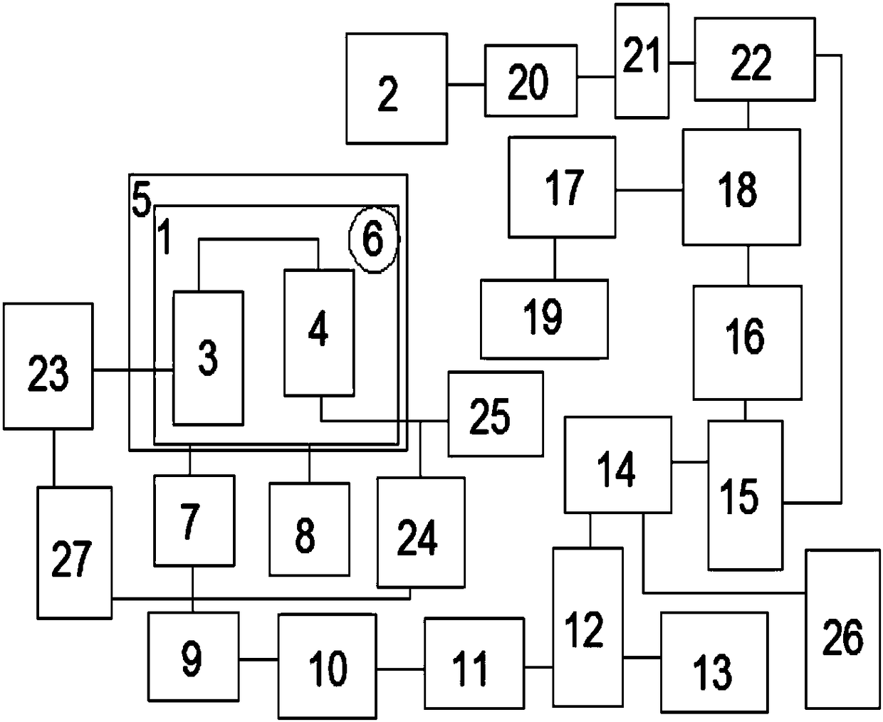
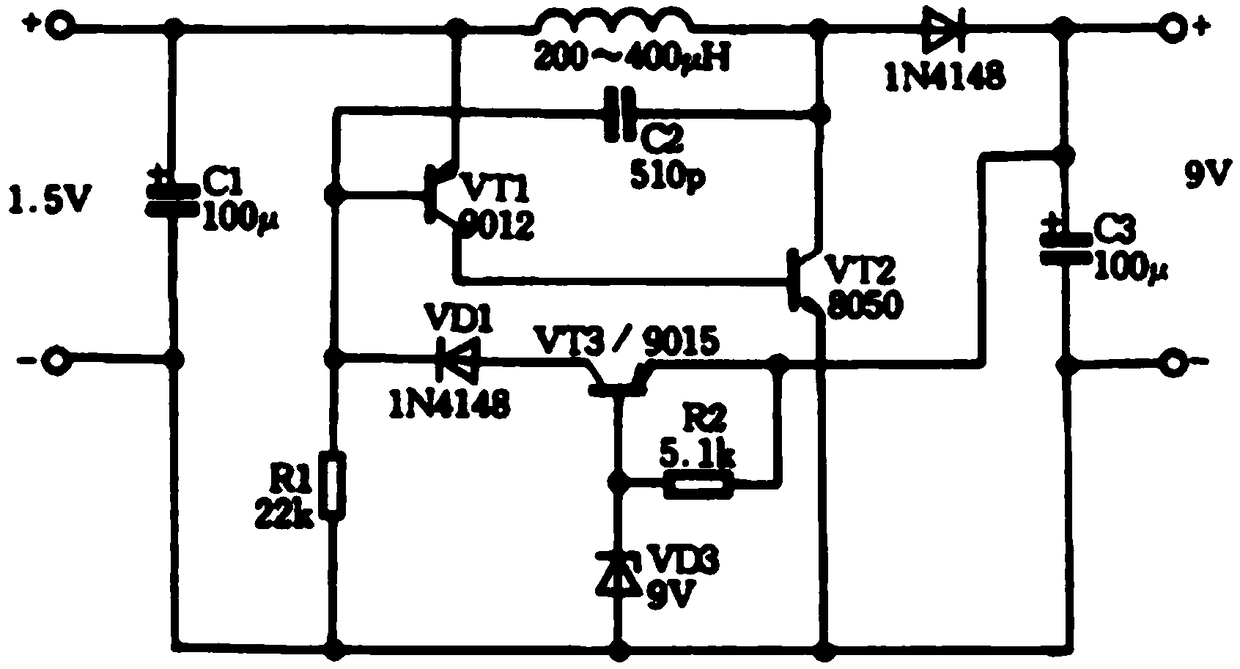
[0014] see figure 1 and figure 2 , the present invention provides a technical solution: a high-frequency and high-speed electronic circuit board based on high-thickness-diameter ratio deep-hole electroplating technology, including a main control board 1 and a signal transmission module 2, and the main control board 1 includes a receiving chip 3 and a driver Chip 4, the communication port of the receiving chip 3 is connected with the driver chip 4 through the control line, and the input terminal of the receiving chip 3 is also connected with the clock control bus 23, and the input terminal of the driver chip 4 is connected with the gate signal respectively. Line 24 is connected with data signal line 25, and strobe signal line 24 is connected with clock control bus 23 through delay circuit 27, and described main control board 1 adopts double-sided flexible circuit board, and outside main control board 1 The surface is also provided with polyester resin material 5, four holes 6...
PUM
 Abstract
Description
Claims
Application Information