

Preparation of hydrotalcite nanosheet/carbon array/metal/silicon combined electrode and application of hydrotalcite nanosheet/carbon array/metal/silicon combined electrode as non-enzymatic sensor
A nanosheet and hydrotalcite technology, which is applied in the field of electrochemical biosensor preparation, can solve the problems of unsuitability for large-scale popularization and application, increased operation difficulty, and many uncertain factors, and achieves good preparation reproducibility and detection stability. , the effect of improving electrical conductivity and improving catalytic activity
- Summary
- Abstract
- Description
- Claims
- Application Information
AI Technical Summary
Problems solved by technology
Method used
Image

Examples
Embodiment 1
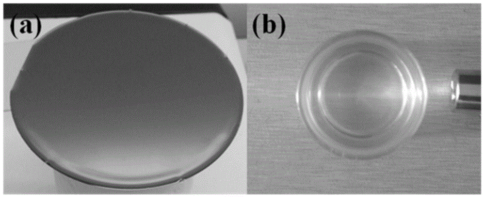
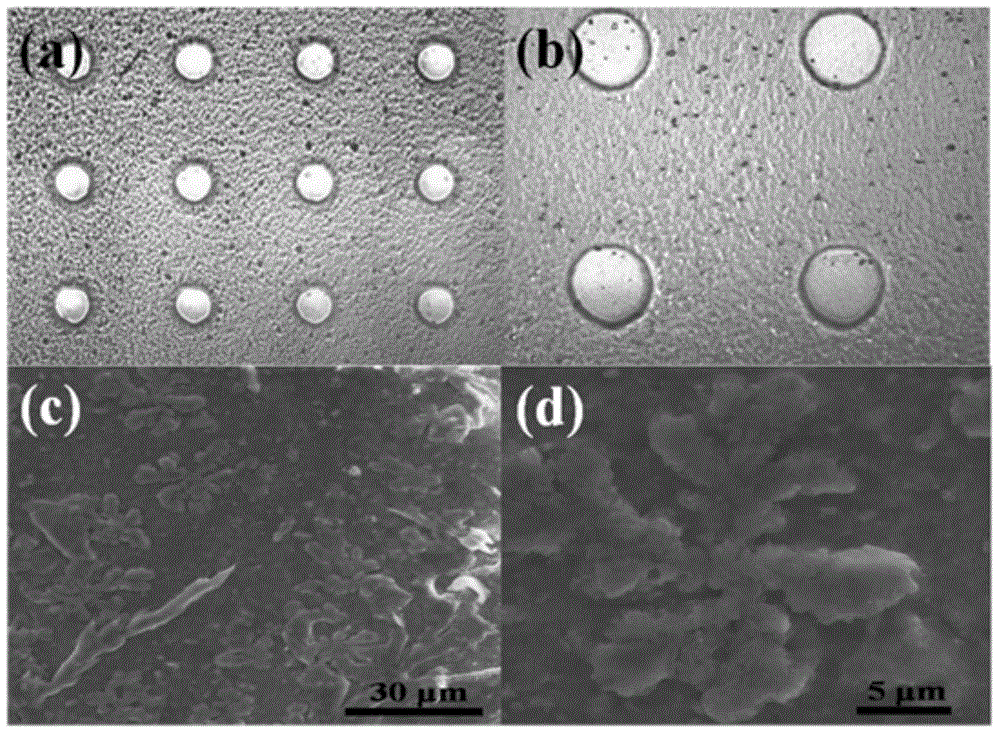
[0034] (1) Place the silicon chip in acetone, ethanol, and secondary water for 20 minutes, rinse with acetone, and use N 2 Blow dry; take the processed silicon wafer as the substrate, use metal sputtering technology, deposit metal platinum under the current condition of 5mA for 120s, obtain a uniform and flat platinum layer on the surface of the silicon wafer, and obtain a platinum / silicon substrate material;
[0035] (2) In the ultra-clean room, use platinum / silicon wafer as the base material, spin-coat SU-8 2050 photoresist with a uniform thickness of 70 μm, and self-levelling for 30 minutes under the conditions of 23 ° C and 50% relative humidity Put it on a rubber drying table for pre-baking, first dry at 65°C for 20 minutes, then dry at 95°C for 30 minutes, and finally cool it for 40 minutes at a temperature of 23°C and a relative humidity of 50% to obtain a photoresist film ;Use a mask plate with neatly arranged light-transmitting regions for exposure, wherein the patter...
Embodiment 2
[0045] (1) Place the silicon chip in acetone, ethanol, and ultrasonic in secondary water for 20 minutes, rinse with acetone, and then wash with N 2 Blow dry; take the processed silicon wafer as the substrate, use metal sputtering technology, deposit metal gold under the current condition of 5mA for 180s, obtain a uniform and flat gold layer on the surface of the silicon wafer, and obtain the gold / silicon substrate material;
[0046] (2) In the ultra-clean room, use gold / silicon wafer as the base material, spin-coat SU-8 2050 photoresist with a uniform thickness of 90 μm, and self-levelling at 23°C and 50% relative humidity for 30 minutes Put it on a rubber drying table for pre-baking, firstly dry it at 65°C for 20 minutes, then dry it at 95°C for 30 minutes, and finally cool it for 30 minutes at a temperature of 23°C and a relative humidity of 50% to obtain a photoresist film ;Use a mask plate with neatly arranged light-transmitting regions for exposure, wherein the pattern of...
Embodiment 3
[0055] (1) Place the silicon chip in acetone, ethanol, and ultrasonic in secondary water for 20 minutes, rinse with acetone, and then wash with N 2 Blow dry; take the processed silicon wafer as the substrate, use metal sputtering technology, deposit metal platinum under the current condition of 5mA for 180s, obtain a uniform and flat platinum layer on the surface of the silicon wafer, and obtain the platinum / silicon substrate material;
[0056] (2) In the ultra-clean room, use platinum / silicon wafer as the base material, spin-coat SU-8 2050 photoresist with a uniform thickness of 80 μm, and self-levelling at 23°C and 50% relative humidity for 30 minutes Put it on a rubber drying table for pre-baking, firstly dry it at 65°C for 20 minutes, then dry it at 95°C for 30 minutes, and finally cool it for 30 minutes at a temperature of 23°C and a relative humidity of 50% to obtain a photoresist film ;Use a mask with neatly arranged light-transmitting regions for exposure, wherein the ...
PUM
 Abstract
Description
Claims
Application Information