Schottky diode manufacturing method and Schottky diode

A Schottky diode and anode technology, applied in semiconductor/solid-state device manufacturing, semiconductor devices, electrical components, etc., can solve problems such as large reverse leakage current, reduce area, reduce reverse leakage current, reduce The effect of a small contact area

Inactive Publication Date: 2017-01-04
PEKING UNIV +2
View PDF2 Cites 6 Cited by
  • Summary
  • Abstract
  • Description
  • Claims
  • Application Information

AI Technical Summary

Problems solved by technology

[0005] Embodiments of the present invention provide a method for manufacturing a Schottky diode and the Schott

Method used


Image

  • Schottky diode manufacturing method and Schottky diode
  • Schottky diode manufacturing method and Schottky diode
  • Schottky diode manufacturing method and Schottky diode

Examples


Example Embodiment

[0036] In order to make the objectives, technical solutions and advantages of the present invention clearer, the present invention will be further described in detail below with reference to the accompanying drawings. Obviously, the described embodiments are only a part of the embodiments of the present invention, rather than all of them. Based on the embodiments of the present invention, all other embodiments obtained by those of ordinary skill in the art without creative work shall fall within the protection scope of the present invention.
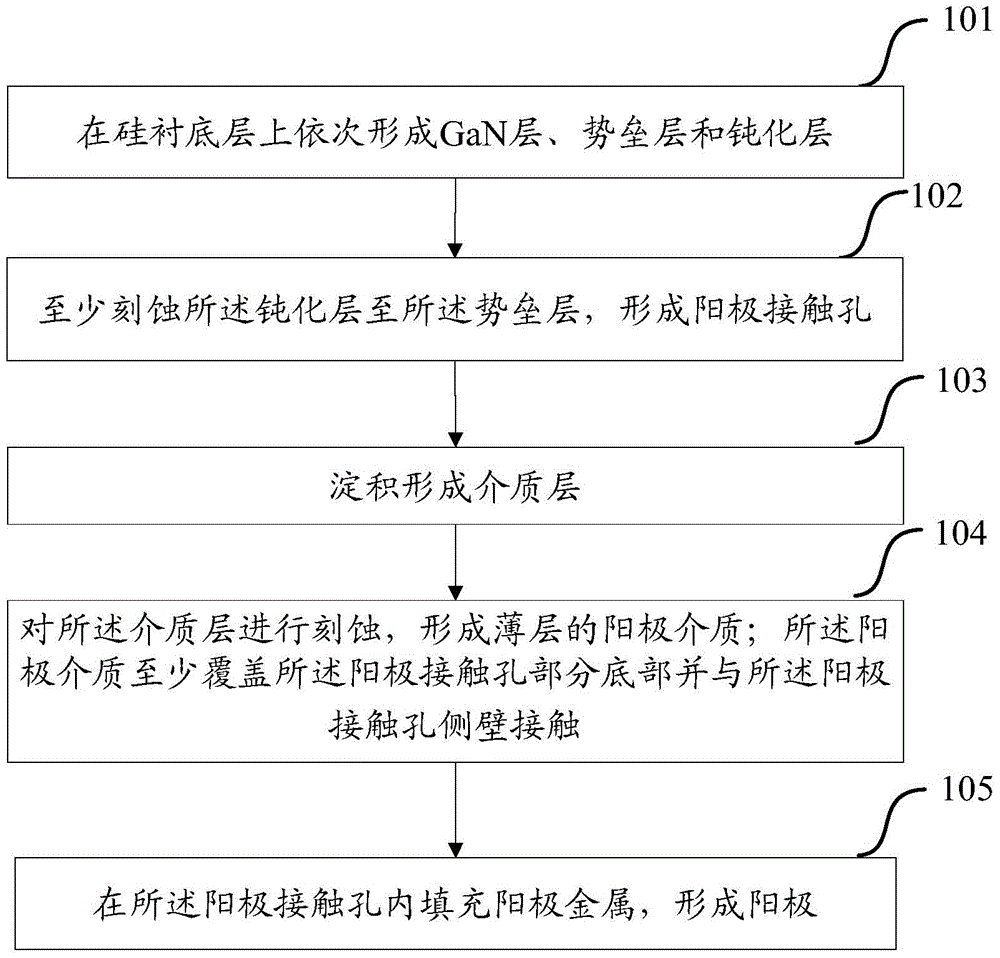
[0037] figure 1 This is a schematic flow diagram corresponding to a method for manufacturing a Schottky diode provided by an embodiment of the present invention, and the method includes:

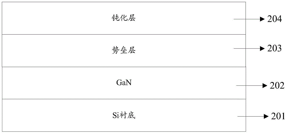
[0038] Step 101, sequentially forming a GaN layer, a barrier layer and a passivation layer on the silicon substrate layer;

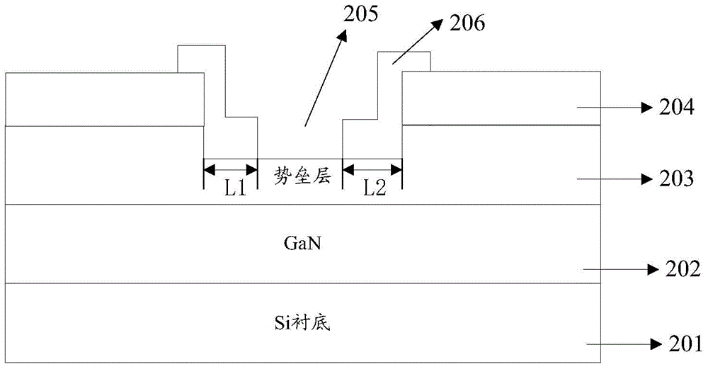
[0039] Step 102, etching at least the passivation layer to the barrier layer to form an anode contact hole;

[0040] Step 103, depositi...


PUM


Abstract

An embodiment of the invention discloses a schottky diode manufacturing method and a Schottky diode. The method comprises: forming a GaN layer, a barrier layer and a passivation layer on a silicon substrate; at least etching the passivation layer to the barrier layer to form an anode contact hole; forming a dielectric layer, and etching the dielectric layer to form a thin anode dielectric, wherein the anode dielectric at least covers a part of bottom portion of the anode contact hole, and makes contact with the side wall of the anode contact hole; and filling metal in the anode contact hole to form an anode. The anode dielectric is formed at the edge of the anode; the anode dielectric reduces contact area of the metal and an AlGaN layer, that is, the area of a schottky junction is reduced, thereby reducing reverse leakage current of the Schottky diode; and besides, the anode dielectric also prevents electric leakage due to defect of the contact surface between the metal and the passivation layer, and thus reverse leakage current of the Schottky diode is further reduced.

Description

technical field [0001] The invention relates to the technical field of semiconductors, in particular to a method for manufacturing a Schottky diode and the Schottky diode. Background technique [0002] With the development of semiconductor technology, power diodes have gradually become a key component in circuit systems. Power diodes are developing in two important directions: (1) ultra-high current, which can be applied to high-temperature arc wind tunnels, resistance welding machines, etc.; (2) ultra-fast and ultra-durable, not only used in rectification occasions, but also used A switching circuit. In order to meet application requirements such as low power consumption, high frequency, high temperature, and miniaturization, consumers are increasingly demanding power diodes with higher withstand voltage, on-resistance, turn-on voltage drop, reverse recovery characteristics, and high-temperature characteristics. [0003] Compared with traditional junction diodes, Schottky...

Claims


Application Information

Patent Timeline
IPC IPC(8): H01L29/872H01L29/06H01L21/336
CPCH01L29/0688H01L29/66143H01L29/872H01L2229/00
Inventor 刘美华康冬亮陈建国林信南
Owner PEKING UNIV
Why Eureka
Try Eureka