A kind of light-emitting diode epitaxial layer and preparation method thereof

A technology of light-emitting diodes and epitaxial layers, applied in semiconductor devices, electrical components, circuits, etc., can solve the problems of affecting the luminous efficiency of light-emitting diodes, affecting the growth efficiency of light-emitting diodes, poor crystal quality of the P-type gallium nitride layer, etc. Preparation time, excellent crystal quality, and the effect of enhancing luminous intensity

Active Publication Date: 2018-12-04
ANHUI SANAN OPTOELECTRONICS CO LTD
View PDF5 Cites 0 Cited by
  • Summary
  • Abstract
  • Description
  • Claims
  • Application Information

AI Technical Summary

Problems solved by technology

In order to obtain a flat surface, the thickness of the unintentionally doped gallium nitride buffer layer and the n-type gallium nitride layer is often about 2.5-3.5 μm, which greatly affects the growth efficiency of light-emitting diodes.
At the same time, in the prior art, the P-type GaN layer is grown on the light-emitting layer, so in order to avoid damage to the light-emitting layer under high temperature conditions, the P-type GaN layer cannot use a higher growth temperature, resulting in P-type The crystal quality of the gallium nitride layer is poor, and it is prone to electrical abnormalities
In addition, growing the P-type GaN layer after the growth of the light-emitting layer is also easy to cause impurities in the P-type GaN layer, usually Mg, to enter the light-emitting layer through diffusion, and on the one hand, destroy the crystal of the light-emitting layer. On the other hand, it is easy to cause non-radiative recombination, which affects the luminous efficiency of light-emitting diodes

Method used


Image

  • A kind of light-emitting diode epitaxial layer and preparation method thereof
  • A kind of light-emitting diode epitaxial layer and preparation method thereof
  • A kind of light-emitting diode epitaxial layer and preparation method thereof

Examples


Embodiment 1

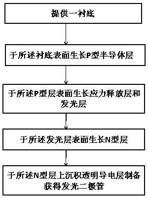
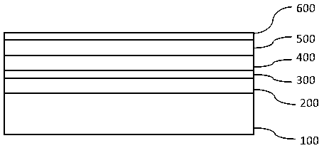
[0030] see Figure 1~2 , the method for preparing the diode epitaxial layer implemented in the present invention will be described in detail below.

[0031] First, a gallium nitride substrate 100 is provided, wherein the gallium nitride substrate 100 is a flat substrate 100 or a patterned substrate 100 .

[0032] Next, put the substrate 100 into the reaction chamber and clean the surface of the substrate 100, adjust the temperature of the chamber to 1000-1200°C, the pressure to 50-100 torr, and adopt low-speed conditions with a rate less than or equal to 0.6 μm / h To grow a P-type gallium nitride layer 200 with a thickness less than or equal to 200 angstroms. In this embodiment, the preferred substrate 100 is a flat substrate 100, and the thickness of the p-type gallium nitride layer 200 is 100-180 angstroms; where the p-type gallium nitride The doping impurity of layer 200 is preferably Mg atom, and because Mg atom has stronger lateral growth ability, so only need to grow thi...

Embodiment 2

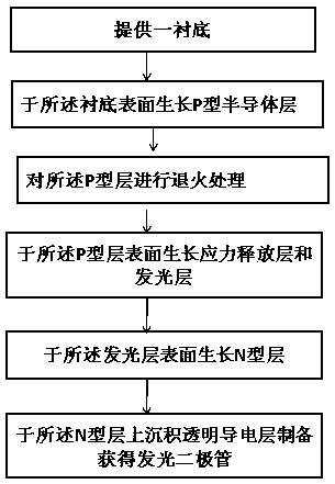
[0037] See attached figure 2 with 3The difference between this embodiment and Embodiment 1 is that this embodiment adds a high-temperature annealing step between the P-type GaN layer 200 and the stress release layer 300, specifically: stop the growth of the P-type GaN layer 200, Stabilize the chamber temperature above 950°C, and perform high-temperature annealing treatment on the P-type GaN layer. The preferred annealing temperature is 950-1100°C, and the annealing time is 1-5 minutes. Use this high-temperature treatment step to activate the P-type gallium nitride layer. The gallium layer is doped with impurities to further increase the impurity concentration entering the light-emitting layer 400 and enhance the luminous efficiency.


PUM

PropertyMeasurementUnit
temperatureaaaaaaaaaa

Abstract

The invention provides a Light emitting diode (LED) epitaxial layer and a preparing method thereof. The method comprises the steps that a P type gallium nitride layer is grown with high temperature condition on the substrate to obtain good crystal quality and then a luminescent layer and an N type gallium nitride layer are grown. Among them, the N type gallium nitride layer is grown with the low temperature condition which has the same growing temperature as the temperature of the barrier layer in the growing luminescent layer, which avoids destroying the quality of the luminescent layer and affecting luminous efficiency.

Description

technical field [0001] The invention relates to the field of semiconductor preparation, in particular to an epitaxial layer of a light emitting diode and a preparation method thereof. Background technique [0002] GaN-based LEDs have extremely broad application prospects in image display, signal indication, lighting, and basic research due to their excellent characteristics such as long life, impact resistance, earthquake resistance, and energy saving, and have become one of the research hotspots in the field of gallium nitride. one. In most of the prior art, an unintentionally doped gallium nitride buffer layer is grown on the substrate, and the n-type gallium nitride layer, the light emitting layer and the p-type gallium nitride layer are continued to be grown after the surface of the buffer layer is flattened. In order to obtain a flat surface, the thickness of the unintentionally doped gallium nitride buffer layer and the n-type gallium nitride layer is often as thick a...

Claims


Application Information

Patent Timeline
Patent Type & Authority Patents(China)
IPC IPC(8): H01L33/32H01L33/00
CPCH01L33/0075H01L33/325
Inventor 林兓兓周瑜张家宏
Owner ANHUI SANAN OPTOELECTRONICS CO LTD
Why Eureka
Try Eureka